Manufacturing method of photomask and photomask
- Summary
- Abstract
- Description
- Claims
- Application Information
AI Technical Summary
Benefits of technology
Problems solved by technology
Method used
Image

Examples
embodiment 1
(Embodiment 1)
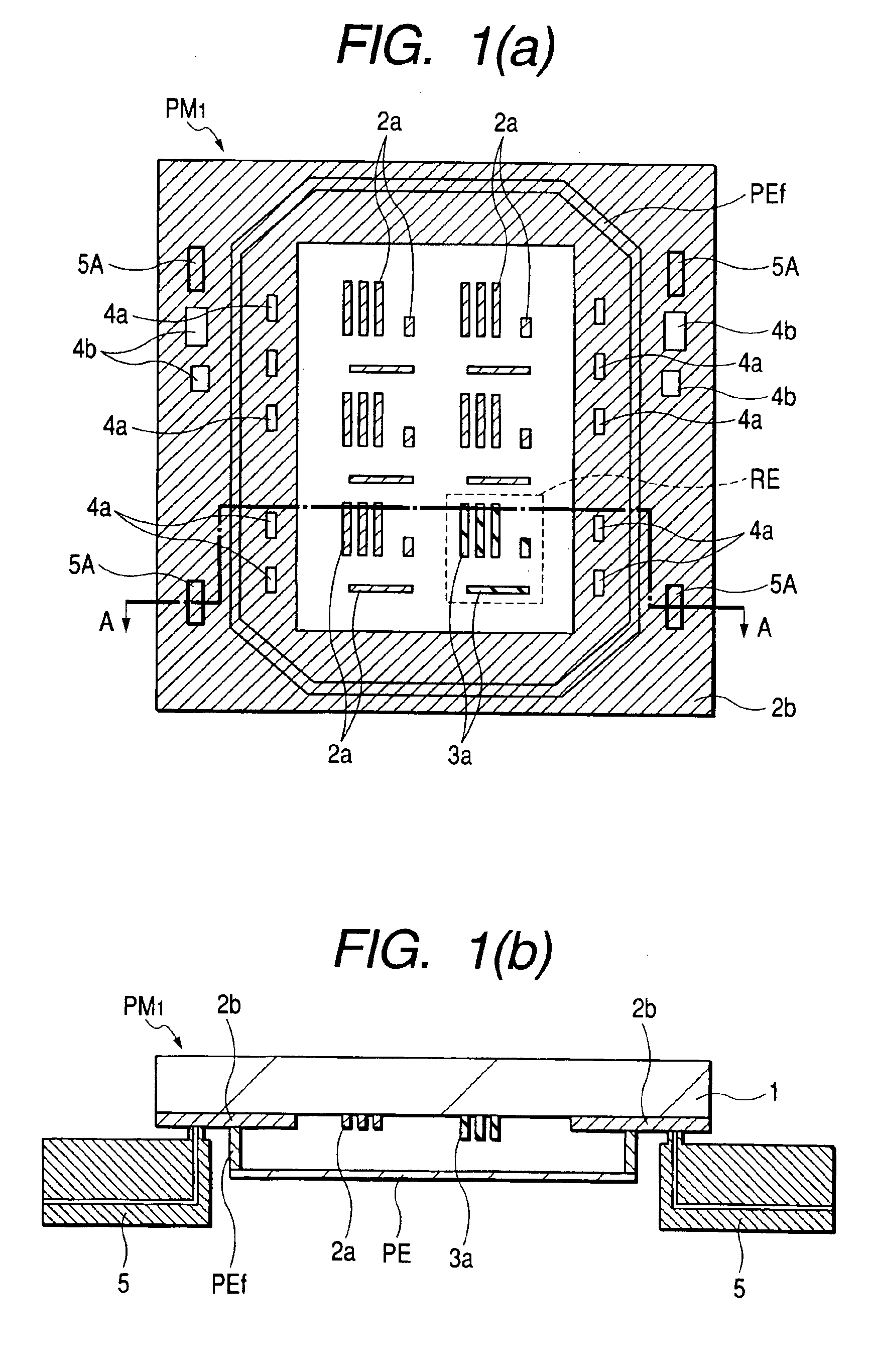
FIG. 1(a) is a plan view showing a photomask according to one embodiment of the present invention, and FIG. 1(b) is a cross-sectional view taken along line A—A of FIG. 1(a) at the time that the photomask is mounted to a predetermined apparatus.
A mask PM1 according to the present embodiment 1 is a reticle for focusing or image-forming an original of an integrated circuit pattern having a size equal to one to ten times the actual or exact size, fore example onto a wafer through a reduction projection optical system or the like. The present drawing illustrates a mask in which the periphery of a semiconductor chip serves as a light-shielding portion and line patterns are formed over the wafer by use of a positive type resist film.
A mask substrate 1 of the mask PM1 is formed of transparent composite quartz glass or the like having a thickness of 6 mm, which is shaped in the form of a plane quadrangle, for example. An optical transmissive opening region shaped in the form of...
embodiment 2
(Embodiment 2)
The present embodiment 2 will describe a modification of a mask. Portions other than it are the same as the embodiment 1.
A mask PM2 shown in FIG. 21 is a mask wherein a peripheral outline of a semiconductor chip serves as a light-shielding portion. A mask wherein a positive type resist film is used over a wafer to form line patterns, is illustrated by way of example. Incidentally, FIG. 21(a) is a plan view of the mask PM2, and FIG. 21(b) is a cross-sectional view taken along line A—A of FIG. 21(a), respectively.
Light-shielding patterns 2a and 3a in an integrated circuit pattern region over the mask PM2 are identical to those employed in the embodiment 1. Patterns transferred onto the wafer through the use of the mask PM2 are identical to those shown in FIGS. 8 and 9 and the like. In the present embodiment, a band or strip light-shielding patterns 2c formed of a metal, for example, are formed over the outer periphery of the integrated circuit pattern region of the mask ...
embodiment 3
(Embodiment 3)
The present embodiment 3 will explain a modification of a mask. Portions other than it are identical to those employed in the embodiment 1.
A mask PM3 shown in FIG. 24 shows, as an example, a mask wherein a negative type resist film is used over a wafer to form line patterns. Incidentally, FIG. 24(a) is a plan view of the mask PM3, and FIG. 24(b) is a cross-sectional view taken along line A—A of FIG. 24(a), respectively.
A main surface of a mask substrate 1 of the mask PM3 is covered with a light-shielding film 2d formed of a metal substantially over the whole surface thereof. The light-shielding film 2d makes use of the same material as the light-shielding patters 2a through 2c referred to above. In element transfer regions D1 through D3 in an integrated circuit pattern of the mask PM3, some of the light-shielding film 2d are removed to form light transmissive patterns 16a. In a region RE lying within the integrated circuit pattern region, the light-shielding film 2d is...
PUM
 Abstract
Description
Claims
Application Information
 - Generate Ideas
- Intellectual Property
- Life Sciences
- Materials
- Tech Scout
- Unparalleled Data Quality
- Higher Quality Content
- 60% Fewer Hallucinations
Browse by: Latest US Patents, China's latest patents, Technical Efficacy Thesaurus, Application Domain, Technology Topic, Popular Technical Reports.
© 2025 PatSnap. All rights reserved.Legal|Privacy policy|Modern Slavery Act Transparency Statement|Sitemap|About US| Contact US: help@patsnap.com