Method and process to make multiple-threshold metal gates CMOS technology

a metal gate and multiple-threshold technology, applied in the field of semiconductor devices, can solve the problems of reducing the effective gate capacitance of the mosfet, reducing the time propagation delay rc of the gate, and affecting the performance of the ga

Inactive Publication Date: 2005-01-25
GLOBALFOUNDRIES U S INC
View PDF9 Cites 117 Cited by
  • Summary
  • Abstract
  • Description
  • Claims
  • Application Information

AI Technical Summary

Benefits of technology

The following example is provided to illustrate some advantages that can be obtained using one of the methods of the present application. In particular, the following example illustrates the use of the second method of the present invention wherein a metal alloy layer is employed.

Problems solved by technology

One disadvantage of utilizing polysilicon gates is that at inversion, the polysilicon gates generally experience depletion of carriers in the area of the polysilicon gate that is adjacent to the gate dielectric.
The depletion effect reduces the effective gate capacitance of the MOSFET.
The decrease in resistance causes a decrease in the time propagation delay RC of the gate.
Although a silicide top gate region may help decrease the resistance of the transistor, charge is still depleted in the vicinity of the interface formed between the bottom polysilicon gate and gate dielectric, thereby causing a smaller effective gate capacitance.
Although metal gates can be used to eliminate the poly-depletion effect and to provide lower gate resistance, it is generally quite difficult to offer multiple-threshold voltages with metal gates.
The prior art does not disclose the use of a bimetal layer in forming one of the silicide regions, nor does it disclose a process where metal alloys are used.
However, carrier mobility is degraded with ever increasing impurity doping which, in turn, degrades the device performance.
The threshold voltage variations due to doping fluctuation will also limit the effectiveness of the doping technique.

Method used


Image

  • Method and process to make multiple-threshold metal gates CMOS technology
  • Method and process to make multiple-threshold metal gates CMOS technology
  • Method and process to make multiple-threshold metal gates CMOS technology

Examples


example

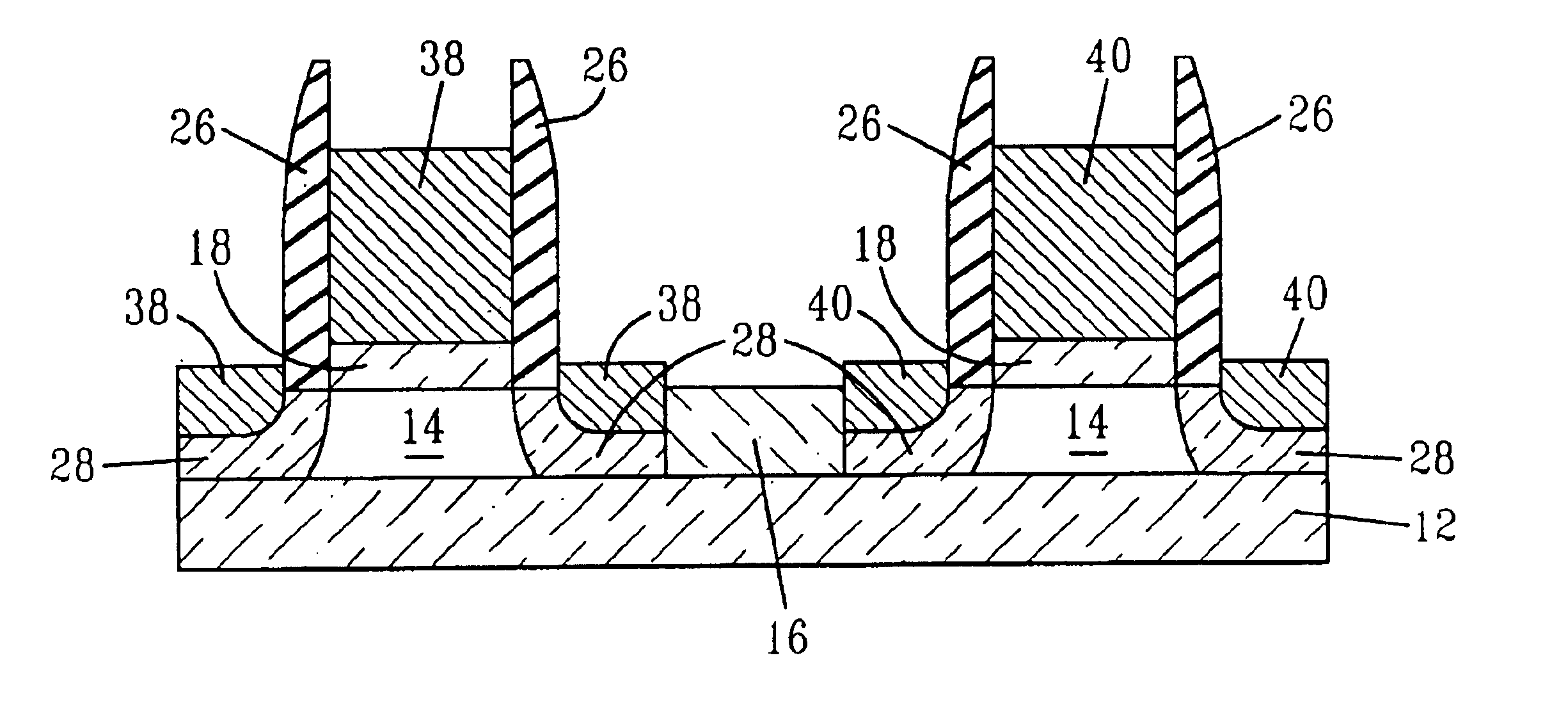
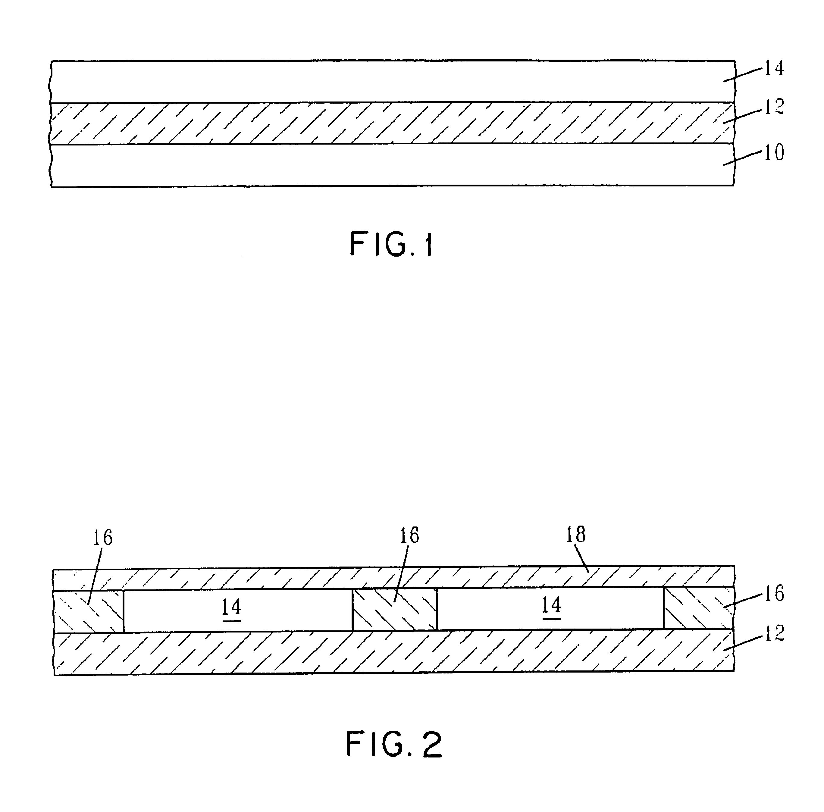
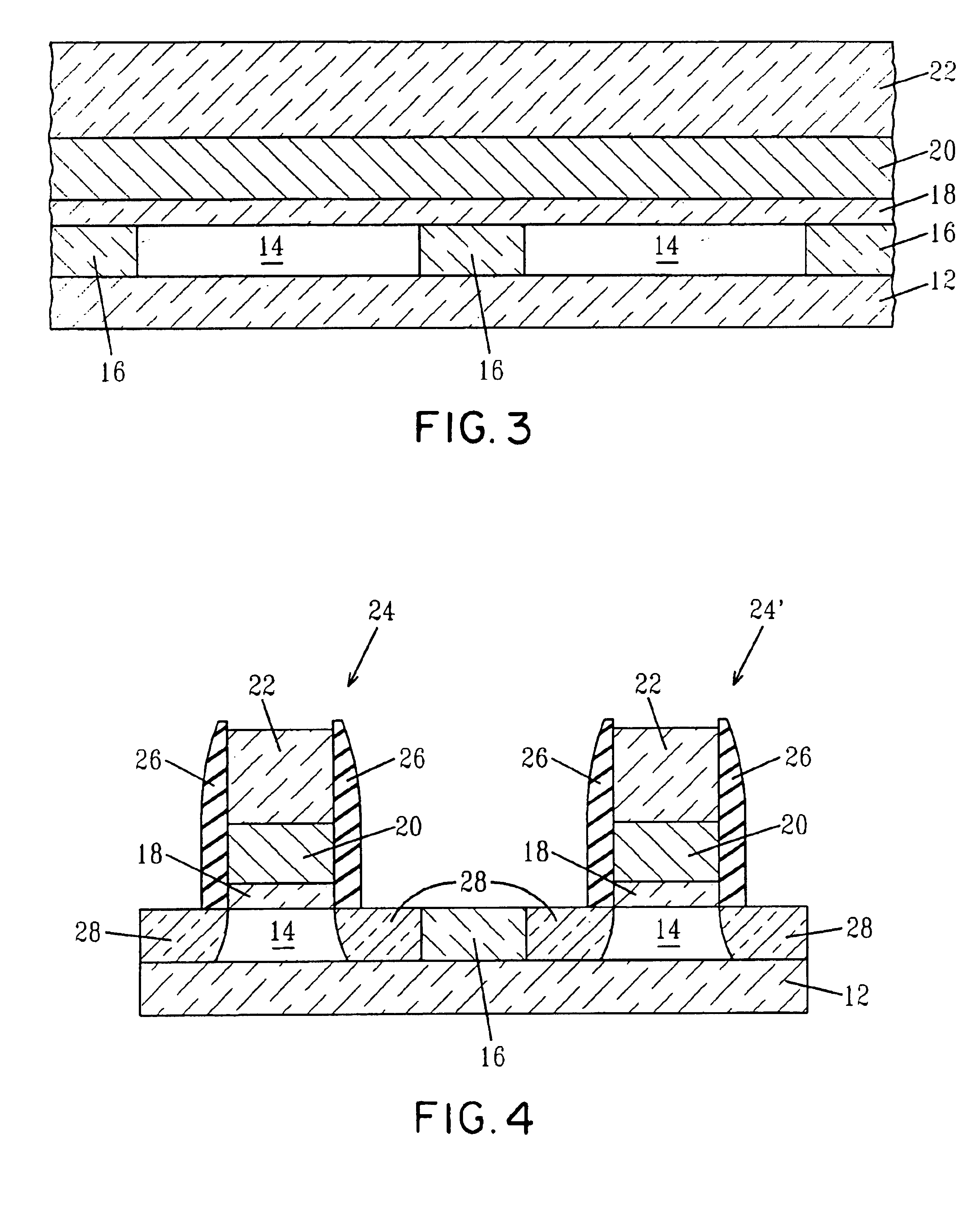
In this example, a Co alloy containing 5% Sn was compared to pure Co using the second method of the present invention. Specifically, a MOSFET structure including a patterned gate stack comprising 40 nm polysilicon gate and a 140 nm capping oxide layer was prepared. The patterned gate stack included 1.4 nm wide oxynitride spacers formed on opposing sidewalls thereof. The oxide capping layer was removed prior to activating the source / drain regions. The threshold voltage for NFET (263 nm gate width) poly-Si control device was 0.4V. When pure Co was used to form the CoSi2, the threshold voltage value was 0.77 V. When Co containing 5 atomic % Sn was employed, the CoSi2(Sn) gate thus formed had a threshold voltage of about 1.02 V (a shift of about 250 mV toward the pFET direction). This example clearly demonstrates that the fully silicide metal alloy gate can effectively adjust the threshold voltage of a MOSFET.


PUM

PropertyMeasurementUnit
temperatureaaaaaaaaaa

Abstract

Methods of forming complementary metal oxide semiconductor (CMOS) devices having multiple-threshold voltages which are easily tunable are provided. Total salicidation with a metal bilayer (representative of the first method of the present invention) or metal alloy (representative of the second method of the present invention) is provided. CMOS devices having multiple-threshold voltages provided by the present methods are also described.

Description

FIELD OF THE INVENTIONThe present invention relates to semiconductor devices, and more particularly to methods for forming complementary metal oxide semiconductor (CMOS) devices which include metal gates having multiple-threshold voltages Vt associated therewith.BACKGROUND OF THE INVENTIONIn current metal oxide semiconductor field effect transistors (MOSFETs), a polysilicon gate is typically employed. One disadvantage of utilizing polysilicon gates is that at inversion, the polysilicon gates generally experience depletion of carriers in the area of the polysilicon gate that is adjacent to the gate dielectric. This depletion of carriers is referred to in the art as the polysilicon depletion effect. The depletion effect reduces the effective gate capacitance of the MOSFET. Ideally, it is desirable that the gate capacitance of the MOSFET be high since high gate capacitance typically equates to more charge being accumulated. As more charge is accumulated in the channel, the source / drain...

Claims


Application Information

Patent Timeline
Patent Type & Authority Patents(United States)
IPC IPC(8): H01L21/02H01L21/28H01L21/70H01L21/8238H01L21/336H01L21/84H01L27/092
CPCH01L21/28097H01L21/823835H01L21/823842H01L29/66545H01L21/84H01L27/092
Inventor AMOS, RICKYBARMAK, KATAYUNBOYD, DIANE C.CABRAL, JR., CYRILLEONG, MEIKEIKANARSKY, THOMAS S.KEDZIERSKI, JAKUB TADEUSZ
Owner GLOBALFOUNDRIES U S INC
Why Eureka
Try Eureka