Electron-emitting device, electron source, image-forming apparatus, and method for producing electron-emitting device and image forming apparatus

a technology of electron emitting device and image forming apparatus, which is applied in the manufacture of electrode systems, lighting and heating apparatuses, and electric discharge tubes/lamps. it can solve the problems of power consumption rise and achieve the effect of reducing the difference in electric characteristics and reducing the difference in characteristi

Inactive Publication Date: 2005-02-01
CANON KK
View PDF157 Cites 53 Cited by
  • Summary
  • Abstract
  • Description
  • Claims
  • Application Information

AI Technical Summary

Benefits of technology

Another method for producing the electron source according to the present invention to attain the above mentioned purpose includes the steps of: arranging on the substrate a plurality of electron-emitting devices each having a plurality of fibers mainly made of carbon, and a plural pieces of wire each being electrically connected to at least one of the plurality of electron-emitting devices; applying a voltage to at least a part of the plurality of electron-emitting devices and measuring the electric characteristic of the electron-emitting device to which the voltage has been applied; and reducing the difference in electric characteristic among the plurality of electron-emitting devices based on the measurement result. The step of reducing the difference in characteristic among the above mentioned plurality of electron-emitting devices includes the step of allowing electrons to be emitted from at least one of the plurality of electron-emitting devices under the depressurized condition.
Furthermore, it is preferable that the step of emitting an electron from the above mentioned electron-emitting device is performed under the condition of a gas physically or chemically reactive to the fiber. In this process, the portion where an electric field concentrates in the fiber is made to be reactive for a partial etching process. As a result, the stable and uniform electron-emitting device, electron source, and image-forming apparatus can be produced.

Problems solved by technology

Furthermore, with an increasing number of displayed pixels, power consumption has risen from a large device capacity of the electron-emitting device when it is driven.

Method used


Image

  • Electron-emitting device, electron source, image-forming apparatus, and method for producing electron-emitting device and image forming apparatus
  • Electron-emitting device, electron source, image-forming apparatus, and method for producing electron-emitting device and image forming apparatus
  • Electron-emitting device, electron source, image-forming apparatus, and method for producing electron-emitting device and image forming apparatus

Examples


embodiments

(Embodiments)

Described below in detail are practical embodiments according to the present invention.

first embodiment

(First Embodiment)

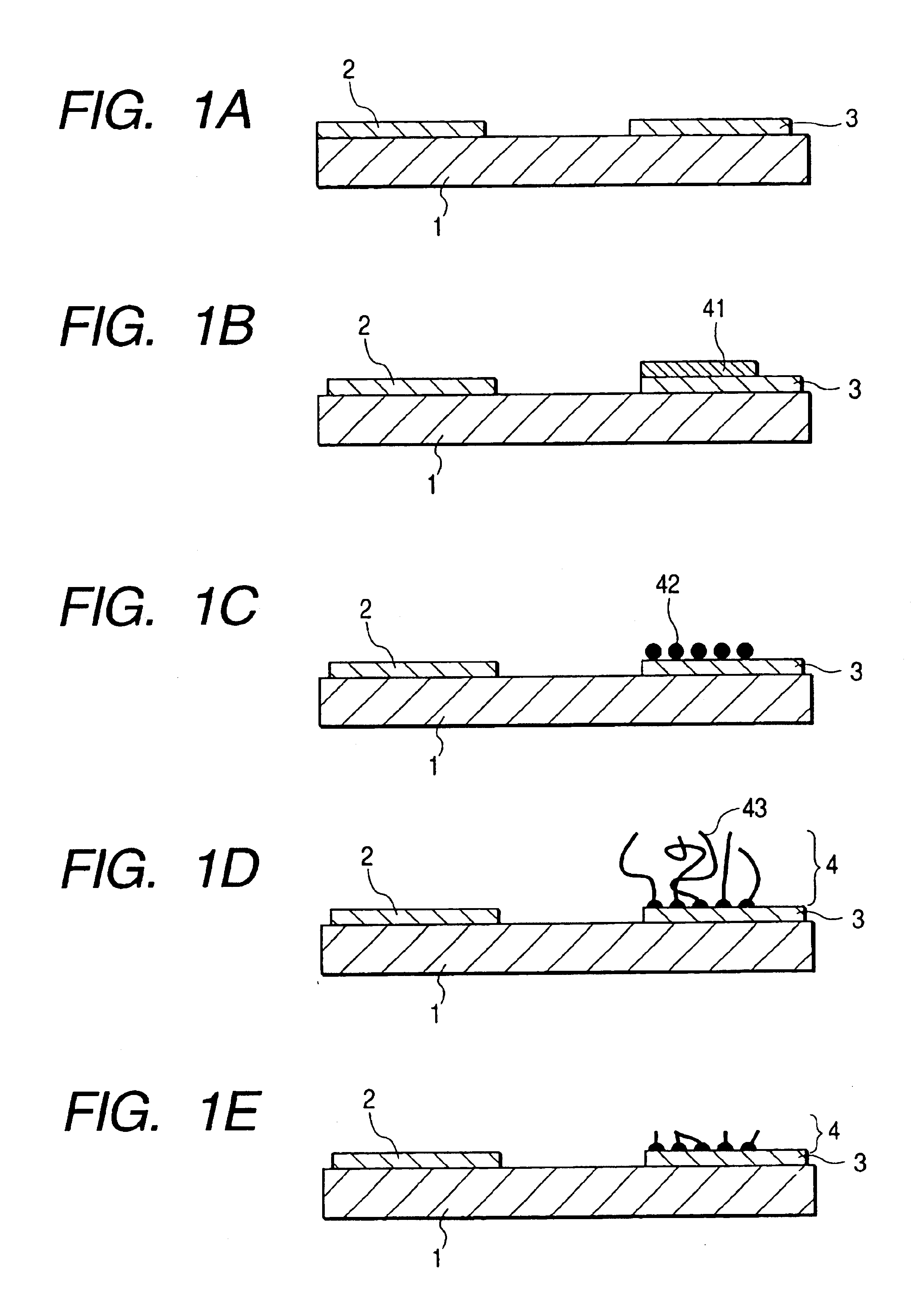
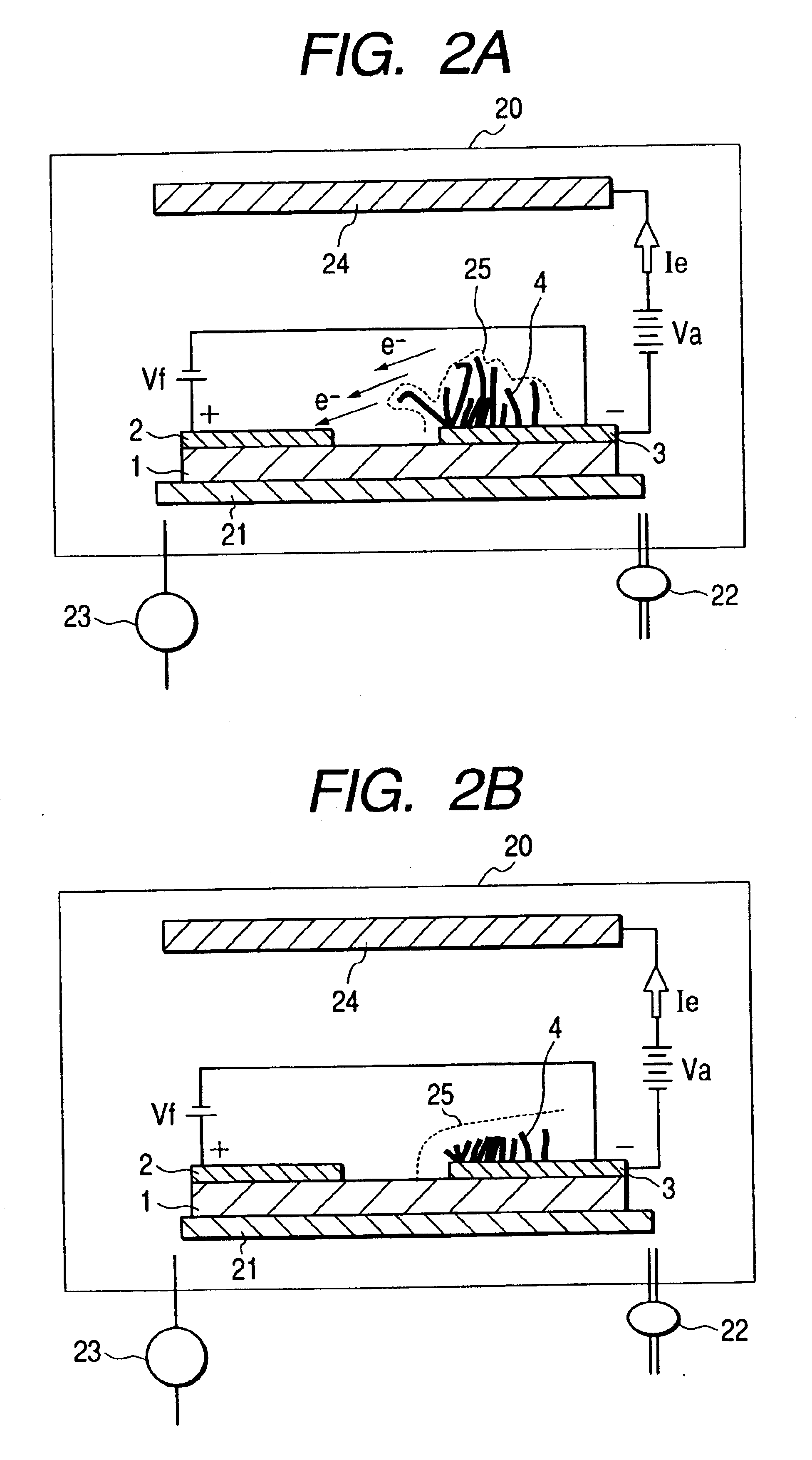
As the first embodiment of the present invention, an electron is emitted between the cathode electrode and the extraction electrode of the electron-emitting device under the condition of an O2 gas, and the “equalizing process” is performed. FIGS. 1A to 1E show a method of producing an electron-emitting device according to the present embodiment. FIGS. 3A and 3B are a plan view and a sectional view of the produced electron-emitting device. Described below is the step of producing the electron-emitting device according to the present embodiment.

(Step 1 (FIG. 1A))

A quarts substrate is cleaned and used as the substrate 1. 5 nm thick Ti and 30 nm thick Pt area are continuously evaporated in the spatter method as the extraction electrode 2 and the cathode electrode 3.

Then, in the photolithography process, a resist pattern is formed using a positive type photoresist (AZ 1500 made by Clariant).

Next, the Pt layer and Ti layer dry etching processes are performed using Ar wit...

second embodiment

(Second Embodiment)

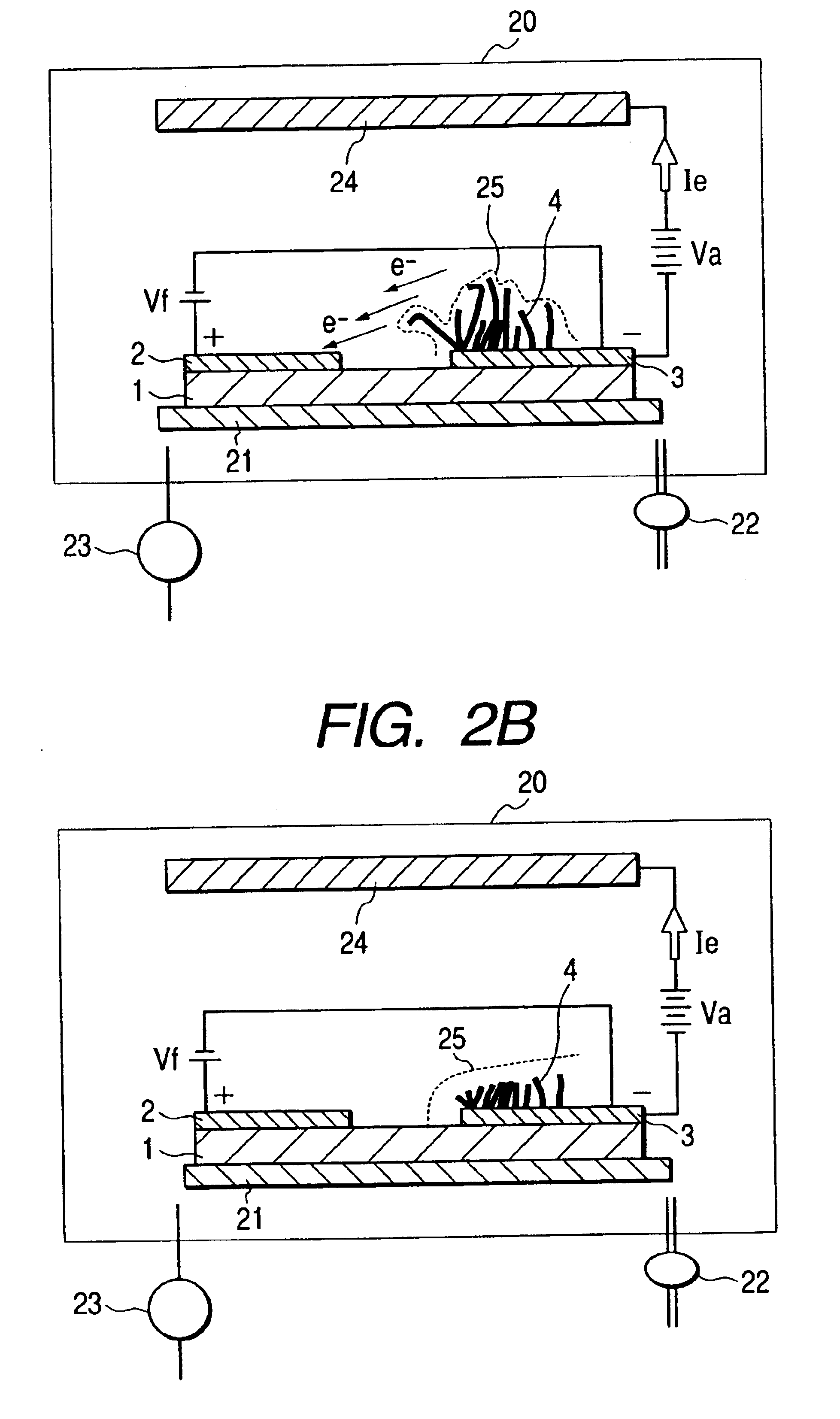
An example of the equalizing process performed by emitting an electron as biased between the cathode electrode of the electron-emitting device and the anode opposing the electron-emitting device in the O2 gas in the second embodiment.

(Step 1)

In the method similarly used in the steps 1 to 4 according to the first embodiment, the extraction electrode 2 and the cathode electrode 3 are formed on the substrate 1, and fibrous carbon is produced as the electron-emitting member 4 on the substrate 1.

(Step 2)

The electron-emitting device is provided for the vacuum device 20 as shown in FIGS. 2A and 2B, the evacuation device 23 performs the evacuation process until 2×10⁻⁶ Pa is reached, the gas leading valve 22 leads the O2 gas until the vacuum level in the vacuum device 20 reaches 1×10⁻⁴ Pa, and the pulse voltage of Vf=20 V (with the pulse width of 10 msec and the pulse length of 4 msec) is applied to the cathode electrode 3 of the electron-emitting device with the extractio...


PUM


Abstract

A method for producing a durable electron-emitting device having a uniform electron emission characteristic, an electron source, and an image-forming apparatus having a uniform display characteristic for a long period are provided. The method for producing an electron-emitting device according to the present invention includes the steps of: disposing a cathode electrode on a surface of a substrate; providing an electrode opposite the cathode electrode; disposing plural pieces of fiber containing carbon as a main component on the cathode electrode; and applying potential higher than potential applied to the cathode electrode under depressurized condition to an electrode opposite the cathode electrode.

Description

BACKGROUND OF THE INVENTION1. Field of the InventionThe present invention relates to an electron-emitting device, an electron source using therewith, an image-forming apparatus, and a method for producing an electron-emitting device.2. Related Background ArtA field emission type (FE-type) electron-emitting device for emitting an electron from a metal surface with a strong field over 106 V / cm applied to the metal has attracted attention as one of the effective cold electron sources.If an FE-type cold electron source is put to practical use, a thin-type emissive image display device can be realized, thereby contributing to a power saving and lightweight system.FIG. 12 shows a vertical FE-type structure. In FIG. 12, reference numeral 121 denotes a substrate, reference numeral 123 denotes an emitter electrode, reference numeral 124 denotes an insulation layer, reference numeral 125 denotes an emitter, reference numeral 126 denotes an anode, and reference numeral 127 denotes the shape of...

Claims


Application Information

Patent Timeline
Patent Type & Authority Patents(United States)
IPC IPC(8): H01J9/02H01J1/304H01J1/30
CPCB82Y10/00H01J1/304H01J9/025H01J31/127H01J1/316H01J2201/30469C01B32/05H01J9/02B82Y40/00
Inventor KITAMURA, SHINTSUKAMOTO, TAKEO
Owner CANON KK
Why Eureka
Try Eureka