Method for manufacturing MTJ cell of magnetic random access memory

a random access memory and cell technology, applied in the field of method for fabricating mtj cells of magnetic random access memory, can solve problems such as difficulty in satisfying current process margins, and achieve the effects of improving yield and productivity, reducing process margins, and improving characteristics

Inactive Publication Date: 2005-02-01
SK HYNIX INC
View PDF1 Cites 4 Cited by
  • Summary
  • Abstract
  • Description
  • Claims
  • Application Information

AI Technical Summary

Benefits of technology

It is an object of the present invention to provide a method for fabricating a MRAM wherein the electric conductivity of a tunnel barrier layer having a thickness 1-10 times greater than that of a conventional tunnel barrier layer is controlled by impurity concentration to obtain sufficient process margin and improve characteristics, reliability, yield and productivity of a device.

Problems solved by technology

As a result, it is difficult to satisfy a current process margin where the thickness variation of the alumina layer allowed within the limit of the resistance variation of a device must be less than 0.1 nm

Method used


Image

  • Method for manufacturing MTJ cell of magnetic random access memory
  • Method for manufacturing MTJ cell of magnetic random access memory
  • Method for manufacturing MTJ cell of magnetic random access memory

Examples


Embodiment Construction

The present invention will be explained in detail referring to the accompanying drawings.

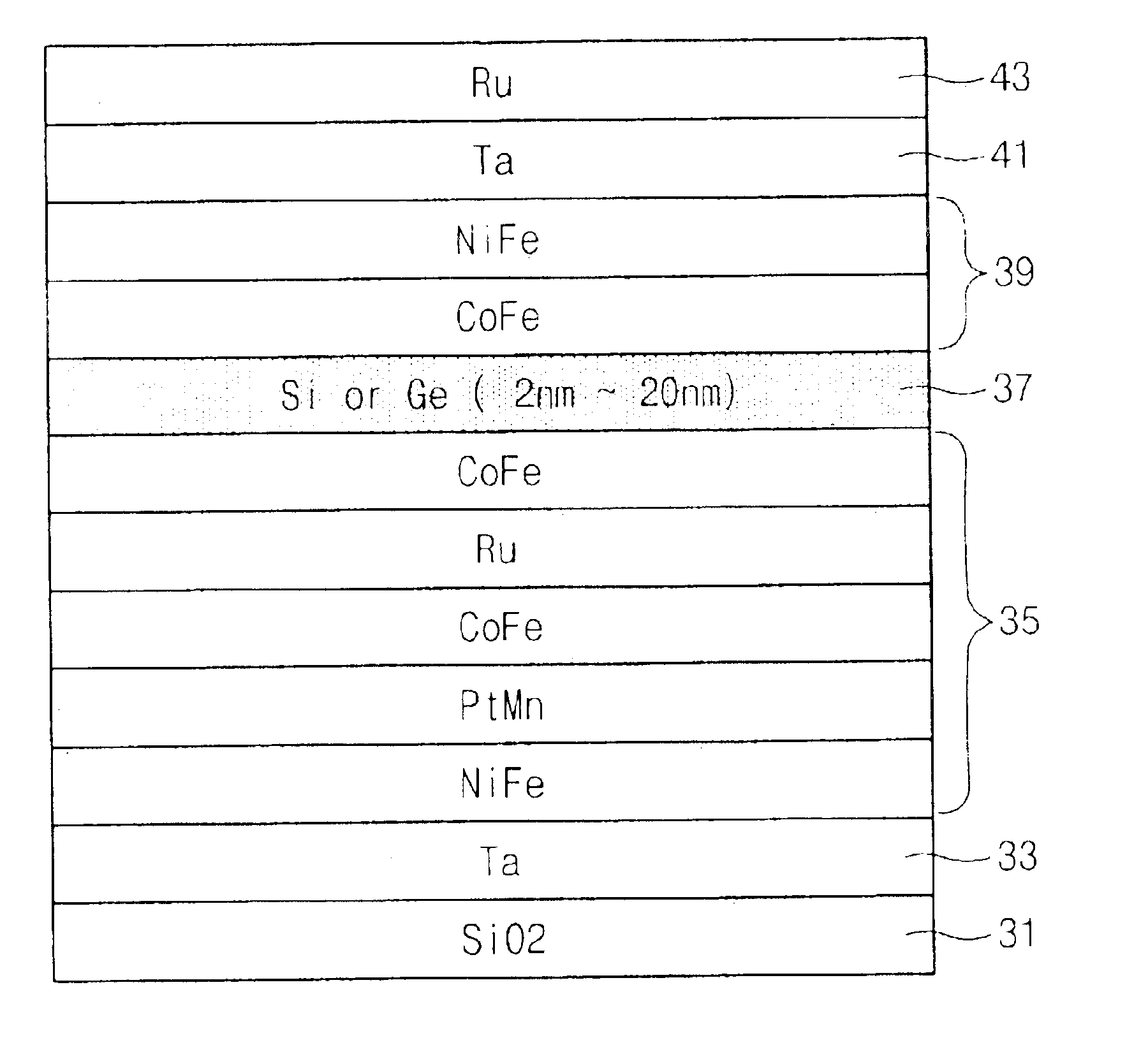
FIG. 4 is a cross-sectional diagram illustrating a MTJ cell of a MRAM according to a preferred embodiment of the present invention.

Referring to FIG. 4, a lower insulating layer 31 is formed on a semiconductor substrate (not shown).

The lower insulating film 31 is an insulating film planarizing the entire surface of the semiconductor substrate having a device isolation film (not shown), a transistor (not shown) comprising a first wordline which is a read line and a source / drain region, a ground line (not shown), a conductive layer (not shown), and a second wordline (not shown) which is a write line thereon.

Then, a connection layer 33 electrically connected to the conductive layer is formed using Ta.

A pinned ferromagnetic layer 35 electrically connected to the connection layer 33 is formed.

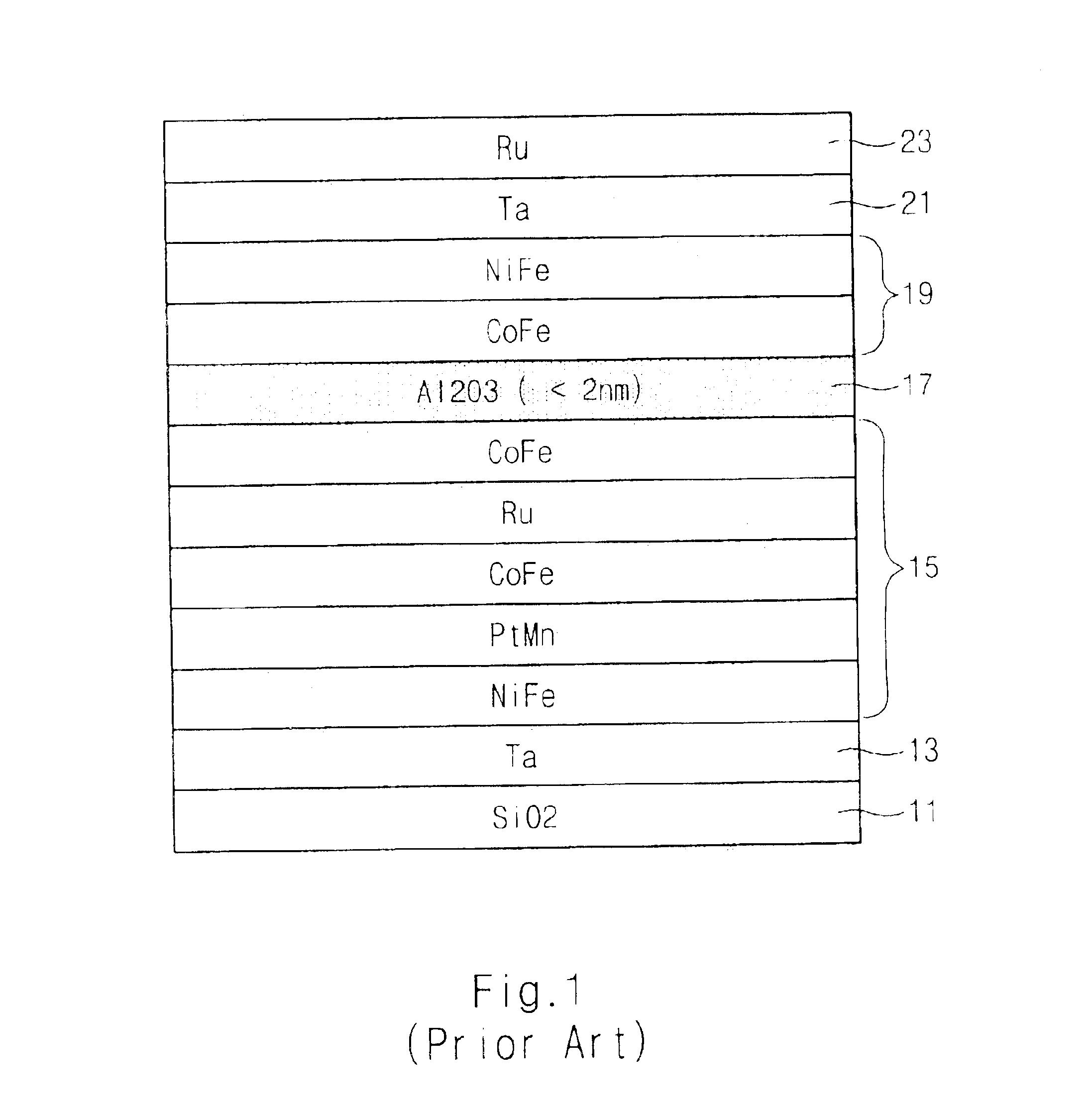
The pinned ferromagnetic layer 35 includes a stacked structure of a NiFe layer, a PtMn layer, a CoFe layer, a ...


PUM


Abstract

A method for fabricating a MTJ cell of a magnetic random access memory (MRAM) using a semiconductor film as a tunnel barrier layer is disclosed. The method comprises the steps of: forming a pinned ferromagnetic layer on a connection layer; forming a tunnel barrier layer using a semiconductor film on the pinned ferromagnetic layer; and forming a free ferromagnetic layer on the tunnel barrier layer.

Description

BACKGROUND OF THE INVENTION1. Field of the InventionThe present invention relates to a method for fabricating a MTJ cell of a magnetic random access memory (hereinafter, referred to as ‘MRAM’), having a higher speed than a SRAM, integration density as high as a DRAM, and a property of a nonvolatile memory such as a flash memory.2. Description of the Prior ArtMost of the semiconductor memory manufacturing companies have developed the MRAM using a ferromagnetic material as one of the next generation memory devices.The MRAM is a memory device for reading and writing information. It has multi-layer ferromagnetic thin films, and operates by sensing current variations according to a magnetization direction of the respective thin film. The MRAM has high speed and low power consumption, and allows high integration density due to the special properties of the magnetic thin film. The MRAM also performs a nonvolatile memory operation similar to a flash memory.The MRAM is a memory device which ...

Claims


Application Information

Patent Timeline
Patent Type & Authority Patents(United States)
IPC IPC(8): H01L21/00H01L27/105H01L43/08G11C11/15H01L21/8246
CPCH01L43/08Y10S438/971H10N50/10G11C11/15
Inventor LEE, SEAUNG SUK
Owner SK HYNIX INC
Why Eureka
Try Eureka