Focal surface and detector for opto-electronic imaging systems, manufacturing method and opto-electronic imaging system

a manufacturing method and optoelectronic imaging technology, applied in the field of optoelectronic imaging systems, can solve the problems of reducing the spectral transmission range of the camera or imaging system, requiring complicated optics to achieve a large visual field, and reducing the thickness of the solid state elements, reducing the number of rejects, and reducing the flexibility

Inactive Publication Date: 2005-02-01
ASTRIUM GMBH
View PDF9 Cites 37 Cited by
  • Summary
  • Abstract
  • Description
  • Claims
  • Application Information

AI Technical Summary

Benefits of technology

For thinning the solid state element, the element may be connected to an auxiliary carrier, whereby the auxiliary carrier is or may be removed after thinning, for example. Thus, the thickness of the solid state elements may be substantially reduced and their flexibility substantially increased, thereby resulting in a low number of rejects.
Thinning, or reducing the thickness of the solid state element may be achieved by removal, for example, through grinding, etching, spin etching, chemical mechanical polishing (CMP), or a combination thereof. Depending on the application, it is possible to achieve high removal rates, e.g., with grinding, medium removal rates, e.g., with spin etching, or a very high precision, e.g., with the CMP method.
According to these methods, the solid state element is initially present as a wafer, and the wafer is thereafter or later split into chips, for example, prior to bonding with the carrier substrate. This enables a very cost-...

Problems solved by technology

However, conventional detector technology requires a planar design.
However, these require complicated optics to achieve a large visual field and to reduce distortions.
Correspondingly, the price for a camera or an imaging system for such applications is very high.
The field correctors often restrict the spectral transmission range, which is caused, for example, by the narrow transmissio...

Method used


Image

  • Focal surface and detector for opto-electronic imaging systems, manufacturing method and opto-electronic imaging system
  • Focal surface and detector for opto-electronic imaging systems, manufacturing method and opto-electronic imaging system
  • Focal surface and detector for opto-electronic imaging systems, manufacturing method and opto-electronic imaging system

Examples


Embodiment Construction

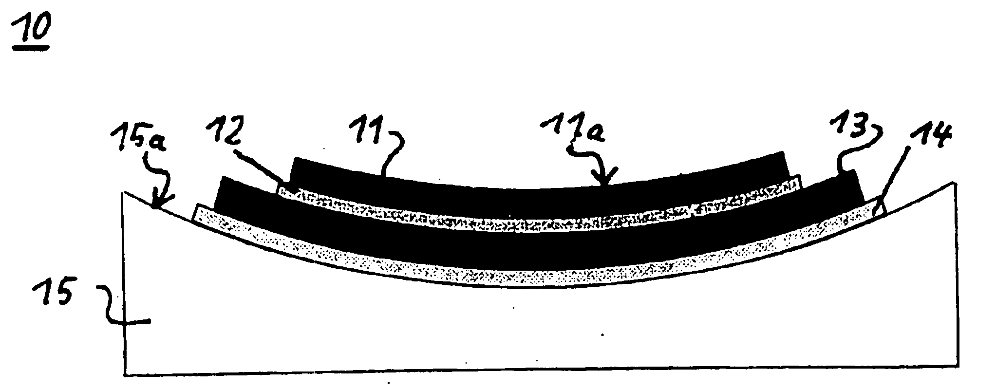
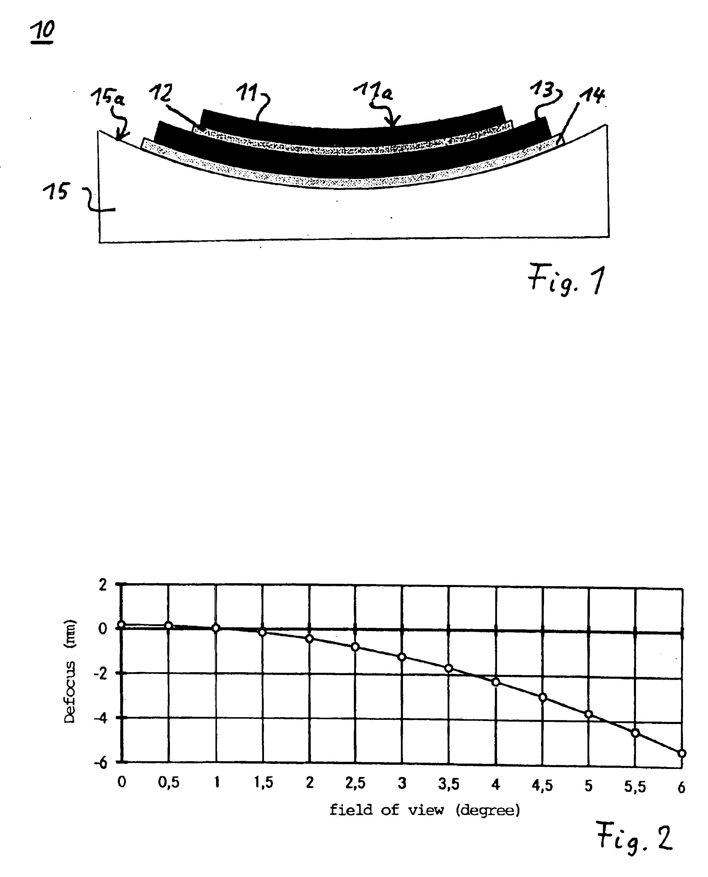
The following describes a first example embodiment of the present invention with reference to FIG. 1. FIG. 1 shows a schematic sectional view through a portion of the focal surface 10. The focal surface 10 includes one or more detectors 11, whereby only one detector 11 in the form of a line sensor is shown in FIG. 1. The detector 11 may be a CMOS line detector with a relatively high length / width ratio that may be, for example, approximately 40. It consists of a chip or a silicon element that is bonded to a flexible carrier substrate 13 via a first bonding layer 12. This first bonding layer 12 may be an adhesive coating that is particularly thin and has a thickness of less than approximately 10 μm, e.g., approximately 1 to 2 μm. The carrier substrate 13 may be made of a flexible foil with a thickness of approximately 50 to 100 μm. The flexible carrier substrate 13 with the chip on it is bonded to a detector carrier 15 by a second bonding layer 14 that is an adhesive coating as well. ...


PUM


Abstract

The focal surface for an opto-electronic imaging system includes an arrangement of detectors for image recording and a detector carrier or a FPA carrier for holding the detectors. The detectors are each made of at least one solid state element that is bonded to a flexible carrier substrate. The focal surface, or the detectors, respectively, exhibits a curvature, such that a curved field of view can be recorded. In a method for manufacturing a focal surface for opto-electronic imaging systems, at least one solid state element is bonded to a flexible carrier substrate to form flexible detectors, whereby a detector carrier provides a curvature and the flexible detectors are adapted to the curvature of the detector carrier. To manufacture a detector according to the present invention, a solid state element is thinned and bonded to a flexible carrier substrate, such that it is formed in a flexible manner and can be adapted to a curvature of a field of view. An opto-electronic imaging system according to the present invention with front optics for capturing an image and a detector arrangement that is arranged in a focal surface of the front optics, in which the detector arrangement is arranged in the focal surface in a curved manner.

Description

FIELD OF THE INVENTIONThe present invention relates to a focal surface for opto-electronic imaging systems, a method for manufacturing a focal surface, a method for manufacturing a detector, a detector and an opto-electronic imaging system.BACKGROUND INFORMATIONOpto-electronic imaging systems are used, for example, in the field of space technology, for earth observation, in reconnaissance systems or in automotive engineering for recognizing obstacles. The sensor head of opto-electronic systems consists of front optics, for example, a lens objective or a telescope, detectors in the focal plane and electronics. The front optics, for example, reflecting telescopes as often used for space instruments have a curved image plane or a curved focal plane. However, conventional detector technology requires a planar design. To flatten the image surface, so-called field correctors or field flatteners must, therefore, be connected downstream of the telescopes or optics in order to be able to pla...

Claims


Application Information

Patent Timeline
IPC IPC(8): H01L27/146G03B15/00G02B23/06G02B23/12H01L27/14H04N5/335
CPCH01L27/14603H01L27/14683H01L27/14625H01L27/1462
Inventor ANSORGE, FANKCRAUBNER, SIEGFRIEDFEIL, MICHAELPLATZ, WILLIRIEDEL, HELMUT
Owner ASTRIUM GMBH
Why Eureka
Try Eureka