Preparation of composite high-K/standard-K dielectrics for semiconductor devices

Inactive Publication Date: 2005-02-01
GLOBALFOUNDRIES INC
View PDF23 Cites 22 Cited by
  • Summary
  • Abstract
  • Description
  • Claims
  • Application Information

AI Technical Summary

Benefits of technology

Thus, the present invention provides a solution to the problem of forming a high-K dielectric material which both overcomes and takes advantage of previously disfavored reactions between dielectric materials, to form a co

Problems solved by technology

Unfortunately, thin oxide films may break down when subjected to an electric field, particularly for gate oxides less than 20 Å thick.
In this manner, a tunneling current may undesirably form between the semiconductor substrate and the gate conductor, adversely affecting the operability of the device.
Breakdown of the gate oxide may also occur at even lower values of gate voltage, as a result of defects in the gate oxide.
Such defects are unfortunately more pronounced in relatively thin gate oxides, since any given defect is more likely to have an adverse effect on the function of the gate oxide.
For example, a thin gate oxide often contains pinholes and/or localized voids due

Method used


Image

  • Preparation of composite high-K/standard-K dielectrics for semiconductor devices
  • Preparation of composite high-K/standard-K dielectrics for semiconductor devices
  • Preparation of composite high-K/standard-K dielectrics for semiconductor devices

Examples


Embodiment Construction

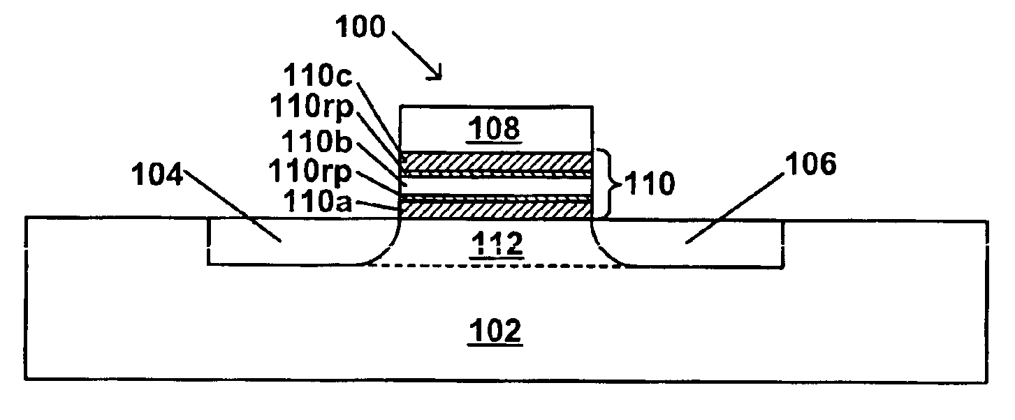
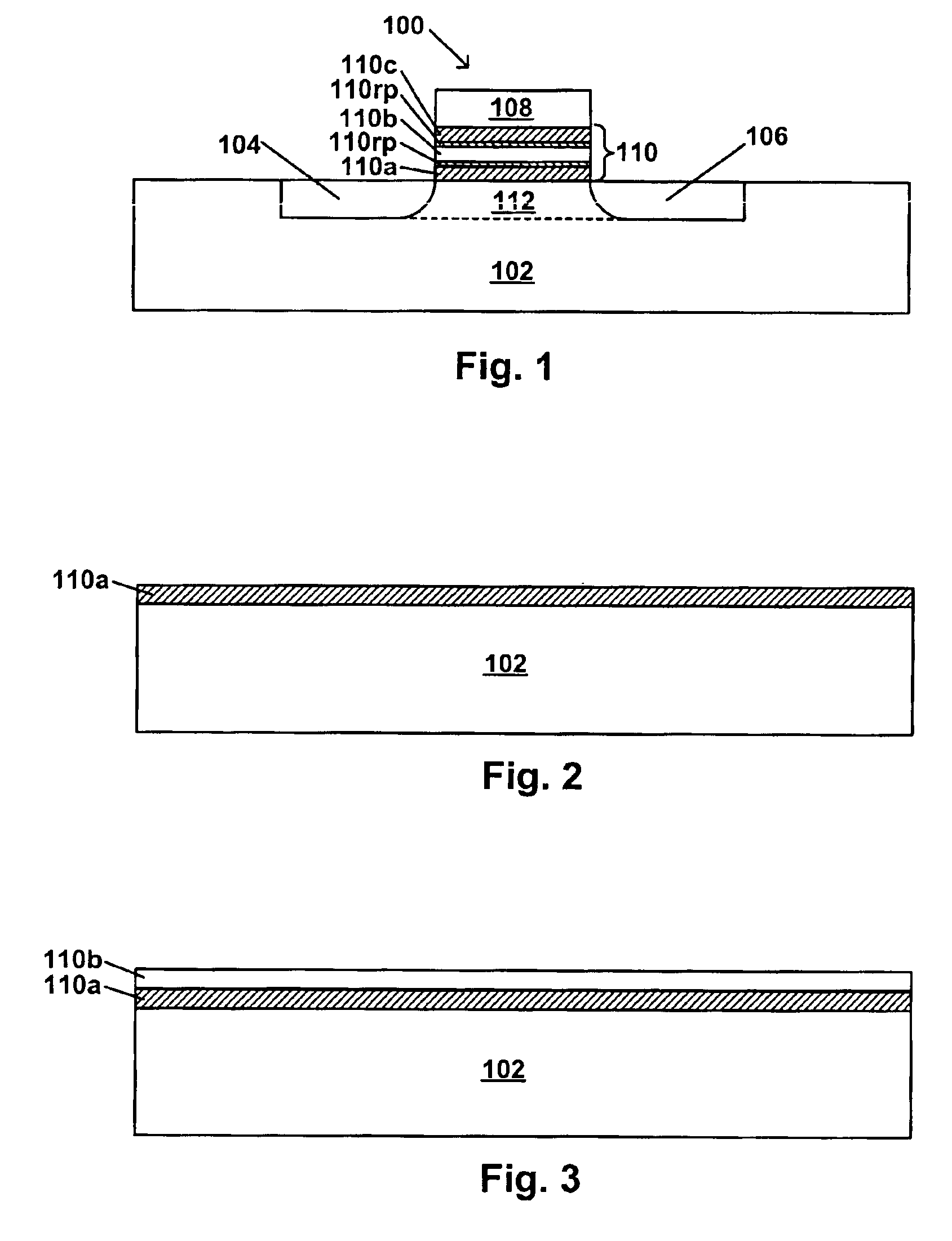
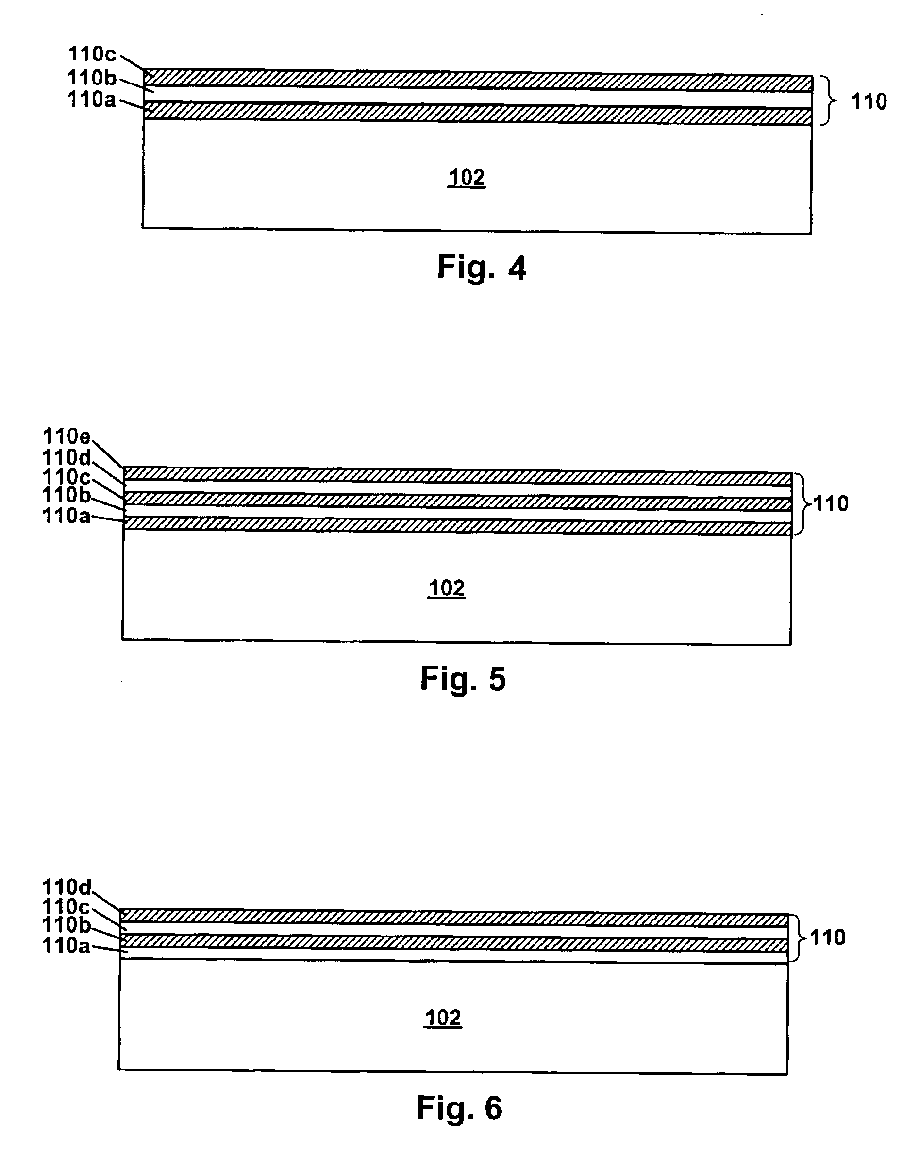
As used herein, the term “standard-K dielectric” refers to a dielectric material having a K up to about 10. Such standard-K dielectric materials include, for example, silicon dioxide, which has a K of about 4, silicon oxynitride, which has a K of about 4-8 depending on the relative content of oxygen and nitrogen, and silicon nitride, which has a K of about 6-9, and aluminum oxide, which has a K of about 10.

As used herein, the term “mid-K dielectric material” refers to a dielectric material having a K in the range from greater than 10 to about 20. Such mid-K dielectric materials include, for example, composite materials such as hafnium silicate, which has a K of about 14, and hafnium silicon oxynitride, which has a K of about 16, depending on the relative content of oxygen and nitrogen, and hafnium silicon nitride, which has a K of about 18.

As used herein, the term “high-K dielectric” refers to a dielectric material having a K of about 20 or more. Such high-K dielectric materials inc...


PUM


Abstract

A semiconductor device having a composite dielectric layer, including a semiconductor substrate, alternating sub-layers including a first dielectric material and a second dielectric material on the semiconductor substrate, the sub-layers forming a composite dielectric layer having at least two sub-layers of at least one of the first dielectric material and the second dielectric material, in which one of the first dielectric material and the second dielectric material is a high-K dielectric material and an other of the first dielectric material and the second dielectric material is a standard-K dielectric material comprising aluminum oxide; and the composite dielectric layer includes a reaction product of the high-K dielectric material and the standard-K dielectric material. In one embodiment, the composite dielectric layer includes a substantially uniform layer of the reaction product of the first dielectric material and the second dielectric material.

Description

FIELD OF THE INVENTIONThe invention relates generally to the fabrication of semiconductor devices and, more particularly, to the fabrication of high-K dielectric layers in semiconductor devices.BACKGROUND OF THE INVENTIONFabrication of semiconductor devices, such as a metal-oxide-semiconductor (MOS) integrated circuit, involves numerous processing steps. In a semiconductor device, a gate dielectric, typically formed from silicon dioxide (“oxide”), is formed on a semiconductor substrate which is doped with either n-type or p-type impurities. For each MOS field effect transistor (MOSFET) being formed, a gate conductor is formed over the gate dielectric, and dopant impurities are introduced into the substrate to form a source and drain. A pervasive trend in modern integrated circuit manufacture is to produce transistors having feature sizes as small as possible. Many present processes employ features, such as gate conductors and interconnects, which have less than 0.18 μm critical dime...

Claims


Application Information

Patent Timeline
IPC IPC(8): H01L21/02H01L21/28H01L29/40H01L29/51H01L21/316
CPCH01L21/28185H01L21/28194H01L21/28211H01L21/316H01L29/513H01L29/517H01L29/518H01L21/28202H01L2924/0002H01L2924/00H01L21/02145H01L21/02178H01L21/02194H01L21/022H01L21/02255
Inventor HALLIYAL, ARVINDJEON, JOONG S.NGO, MINH VANOGLE, ROBERT B.
Owner GLOBALFOUNDRIES INC
Why Eureka
Try Eureka