Microelectronic assemblies with composite conductive elements

a technology of composite conductive elements and microelectronic assemblies, which is applied in the direction of dielectric characteristics, sustainable manufacturing/processing, and final product manufacturing, etc., can solve the problems of severe strain on electrical elements connecting the chip and the substrate, component shrinkage or contraction, and further movement of the chip relative to the substrate, so as to facilitate the movement of the microelectronic elements, reduce the amount of relatively expensive low-melting alloy, and facilitate the effect of microelectronic elemen

Inactive Publication Date: 2005-02-01
TESSERA INC
View PDF26 Cites 10 Cited by
  • Summary
  • Abstract
  • Description
  • Claims
  • Application Information

AI Technical Summary

Benefits of technology

Typically, the microelectronic elements have a normal operating temperature range and the melting temperature of said conductive material is within or below this normal operating temperature range, or only slightly above such range. Therefore, during operation of the assembly, the conductive material wholly or partially liquefies. The cores desirably have melting temperatures well above the operating temperature range of the microelectronic elements, so that the material constituting the cores remains solid during normal operation. The liquid conductive material allows movement of the cores relative to the microelectronic elements, and allows movement of the microelectronic elements relative to one another. This provides compensation for differential thermal effects and other effects which tend to cause relative movement of the elements during service. For example, the first microelectronic elements may be a semiconductor chip and the second microelectronic element may be a circuit panel or a packaging element which is connected to a circuit panel in service. The molten layers of the composite conductive elements will allow movement of the circuit panel relative to the chip. Moreover, the connection remains fatigue-free.
Typically, the layer of conductive material in each conductive element is about 50 μm or less thick, and the cores are spherical. The thin conductive layer reduces the amount of relatively expensive low-melting alloy required in the assembly. The spherical cores facilitate movement of the microelectronic elements relative to one another when the conductive material is in a molten condition. Although the present invention is not limited by any theory of operation, it is believed that the spherical cores roll on one or both microelectronic elements, and thus act much like miniature bearing balls. The cores can be formed from essentially any material. In a particularly desirable arrangement, the cores may be readily deformable to facilitate vertical or Z-direction movement of the microelectronic elements relative to one another in service. The cores may be solid throughout or else may be hollow. Preferably, the assembly also includes a filler disposed between the microelectronic elements and surrounding the conductive elements. The filler can help to constrain the liquid conductive material when the conductive material is in the molten state. The filler desirably is a compliant material such as a gel, elastomer, foam or mesh so that the filler can deform to accommodate the relative movement of the microelectronic elements.
In a particularly preferred arrangement, the second microelectronic element includes a flexible film having a first surface facing in a first vertical direction toward the first microelectronic element and having a second surface facing in a second vertical direction away from said first microelectronic element. The film has contacts on its first surface, which are connected to contacts on the first microelectronic element by the conductive elements. The film also has contacts on its second surface electrically connected to the first-surface contacts and conductive elements. The second surface contacts may be offset from the first-surface contacts and conductive elements in one or more lateral directions transverse to the vertical directions. In this arrangement, the film can bend or bow to accommodate vertical movement of the second-surface contacts relative to the first microelectronic element. Stated another way, the assembly provides good Z-direction compliance, which facilitates mounting of the assembly and also facilitates testing of the assembly prior to mounting. The first microelectronic element may be a semiconductor chip having a front surface facing toward the film or second microelectronic element.

Problems solved by technology

When operation ceases, the chip and the substrate cool down which causes the components to shrink or contract.
The chip and the substrate can also warp as they are heated and cooled, thereby causing further movement of the chip relative to the substrate.
The repeated expansion and contraction of the elements during operation results in severe strain on electrical elements connecting the chip and the substrate.

Method used


Image

  • Microelectronic assemblies with composite conductive elements
  • Microelectronic assemblies with composite conductive elements
  • Microelectronic assemblies with composite conductive elements

Examples


Embodiment Construction

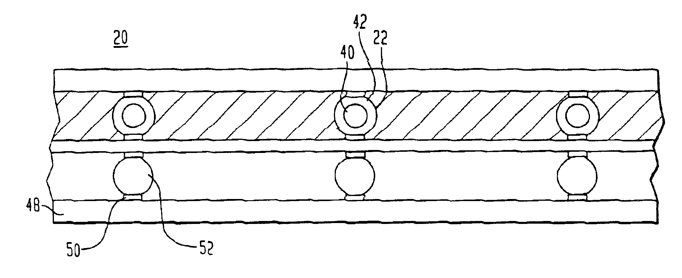
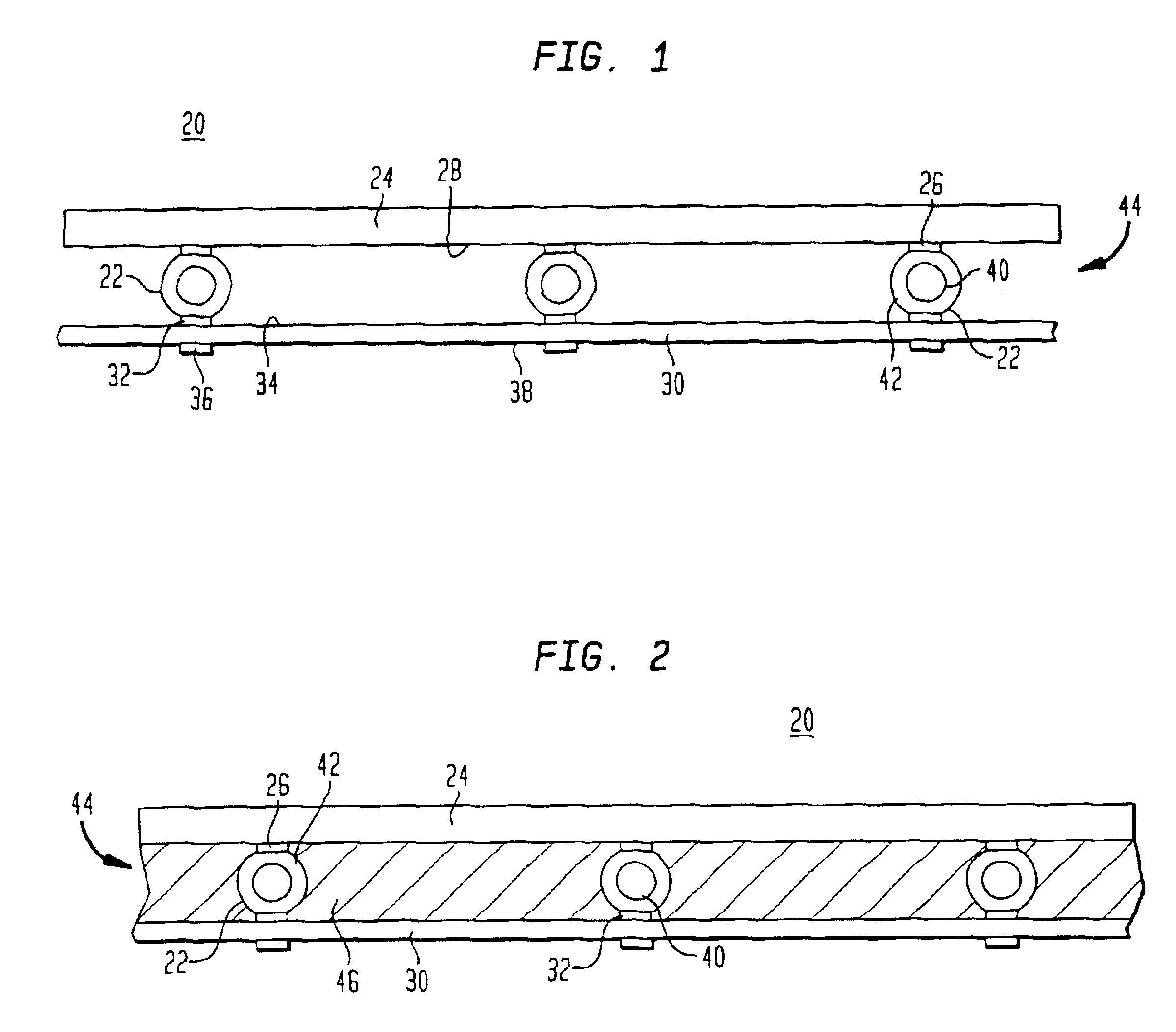
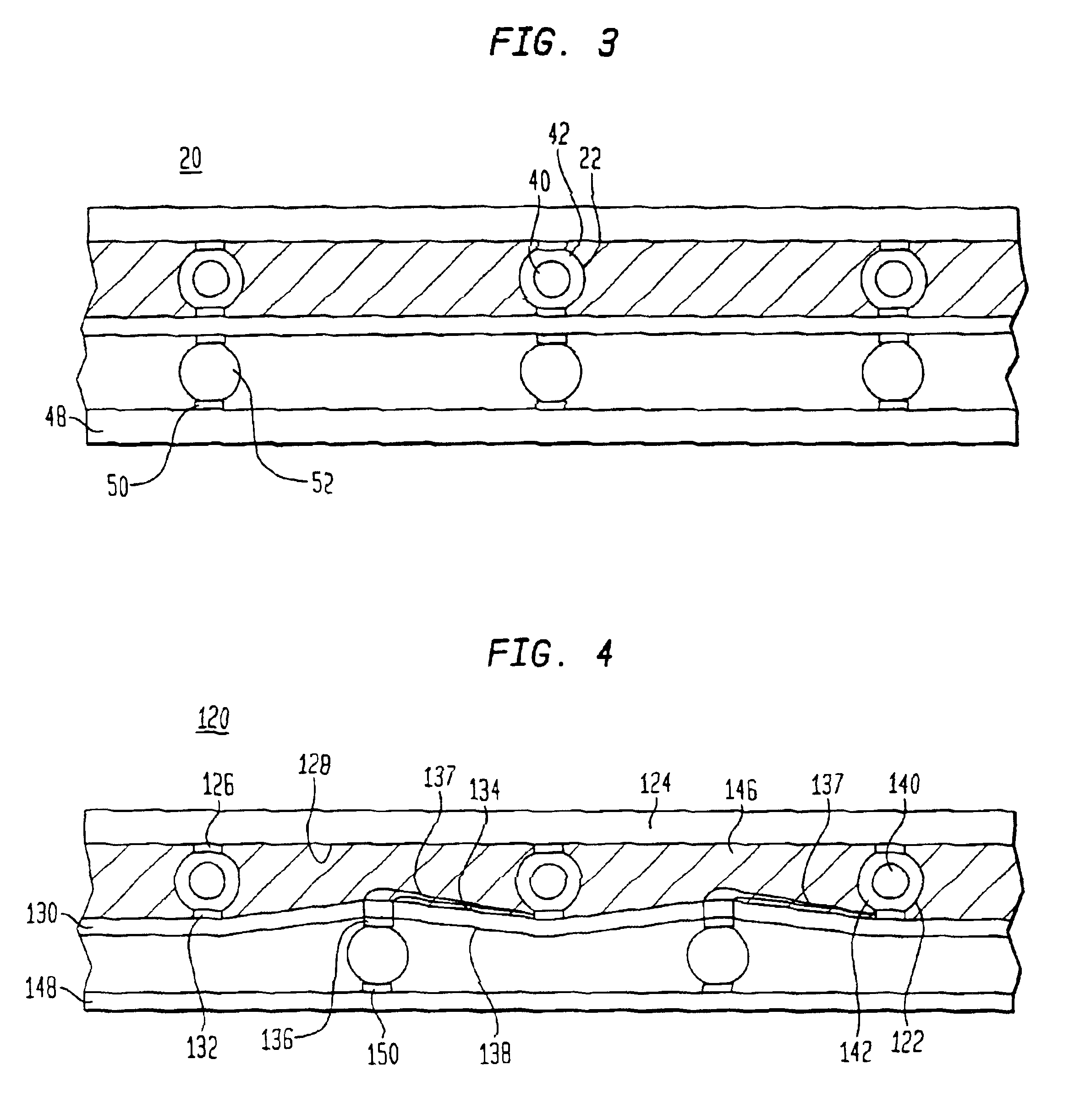
One embodiment of the present invention provides a microelectronic assembly 20 (FIG. 1) having composite conductive elements 22. The microelectronic assembly 20 preferably includes a first microelectronic element 24, such as a semiconductor chip, having a plurality of contacts 26 on a front face 28 thereof. The assembly 20 also includes a second microelectronic element 30, such as a flexible dielectric film, having first contacts 32 on a first surface 34 thereof. The dielectric film 30 may also have second contacts 36 on a second surface 38 thereof which are in registration with the first contacts 32. A plurality of the composite conductive elements 22 are preferably provided over the contacts 32 on the first surface 34 of the dielectric film 30. Each composite conductive element 22 desirably includes a core 40 which is preferably in the shape of a sphere. The core 40 may include a conductive material, such as metal, or a dielectric (non-conductive) material, such as an elastomer. T...


PUM


Abstract

A microelectronic assembly includes composite conductive elements, each incorporating a core and a coating of a low-melting conductive material. The composite conductive elements interconnect microelectronic elements. At the normal operating temperature of the assembly, the low-melting conductive material melts, allowing the cores and microelectronic elements to move relative to one another and relieve thermally-induced stress.

Description

BACKGROUND OF THE INVENTIONThe present invention relates to components and methods for mounting and connecting microelectronic elements such as semiconductor chips.Complex microelectronic devices such as semiconductor chips require numerous connections with other electronic components. Typically such semiconductor chips are mounted on external substrates such as printed circuit boards by electrically interconnecting contacts on the semiconductor chip with contact pads on the substrate. The substrate may include internal circuitry which is connected to the contact pads thereof and may be adapted to accommodate other components such as additional semiconductor chips.Connections between microelectronic elements and substrates must meet several demanding and often conflicting requirements. The connections must provide reliable low impedance electrical interconnections. They must also withstand stresses occurring during manufacturing processes, such as the thermal effects caused by solde...

Claims


Application Information

Patent Timeline
Patent Type & Authority Patents(United States)
IPC IPC(8): H01L21/02H01L21/56H01L23/48H01L23/498H05K1/14H05K3/34
CPCH01L21/563H01L23/49816H01L24/16H05K3/3436H01L2924/00013H01L24/81H01L2224/13099H01L2224/73203H01L2224/812H01L2224/81801H01L2924/01027H01L2924/01029H01L2924/01039H01L2924/01049H01L2924/01082H01L2924/3011H05K1/0271H05K1/141H05K1/147H05K1/189H05K2201/0133H05K2201/10234H05K2201/10378H05K2201/10977H05K2203/128H01L2924/01005H01L2924/01006H01L2924/01033H01L2924/014H01L2224/16238H01L2224/29099H01L2224/05568H01L2224/05573H01L2924/00014Y02P70/50H01L2224/05599
Inventor SMITH, JOHN W.
Owner TESSERA INC
Why Eureka
Try Eureka