Apparatus for capacitor-coupling acceleration

Inactive Publication Date: 2005-02-01
IND TECH RES INST
View PDF8 Cites 13 Cited by
  • Summary
  • Abstract
  • Description
  • Claims
  • Application Information

AI Technical Summary

Benefits of technology

It is therefore an object of the invention to provide an apparatus for capacitor-coupling acceleration in order to reduce the

Problems solved by technology

Unfortunately, interconnect lines are lengthened along with the chip when the chip becomes larger.
Besides, interconnect delays are made larger because greater RC effects result from the smaller line width of the interconnect lines and the narrower space between the interconnect lines.
This approach requires a number of control signals or power supplies, thus resulting in difficulties in implementation.
Thus, the approach is n

Method used


Image

  • Apparatus for capacitor-coupling acceleration
  • Apparatus for capacitor-coupling acceleration
  • Apparatus for capacitor-coupling acceleration

Examples


Example

FIRST EMBODIMENT

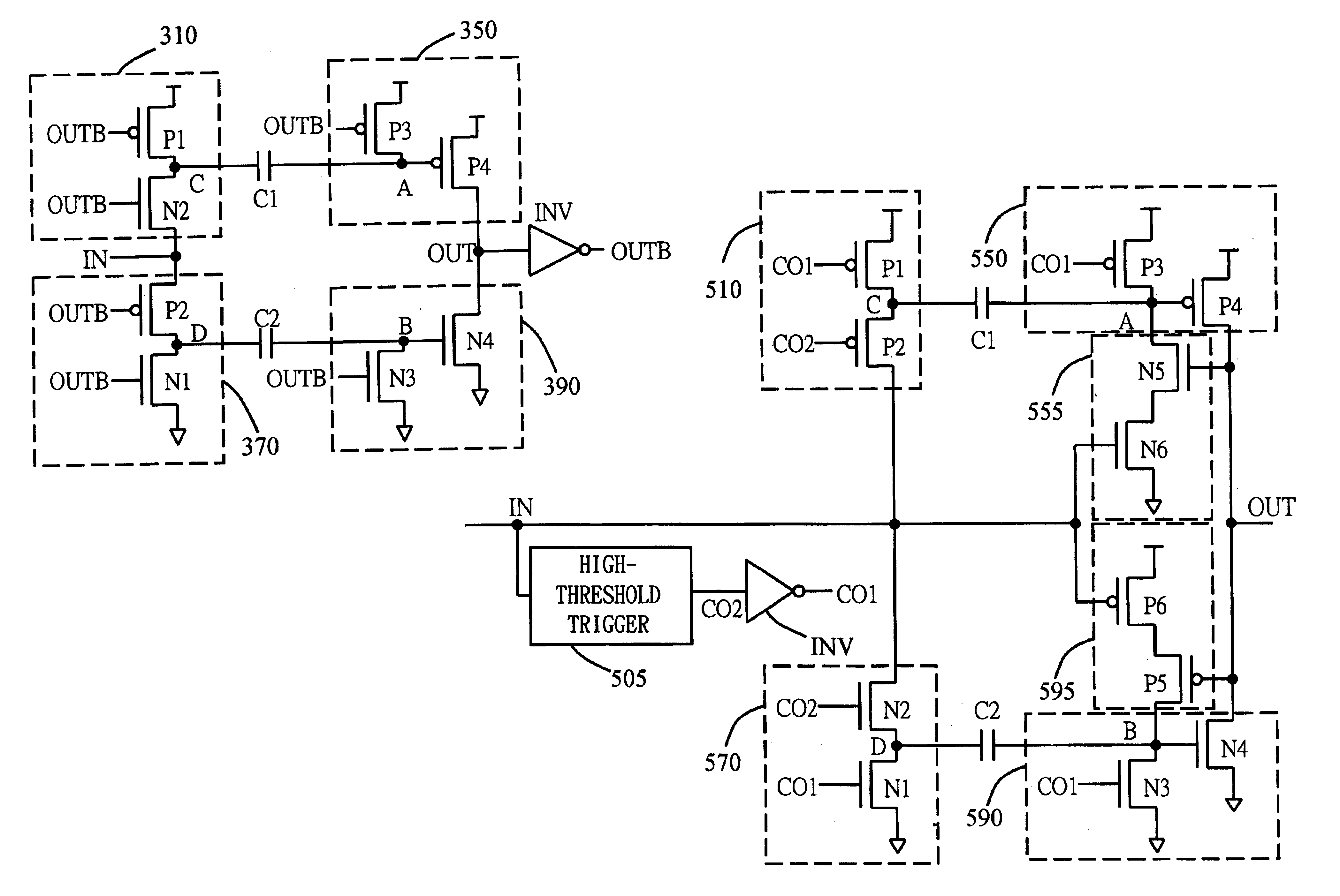
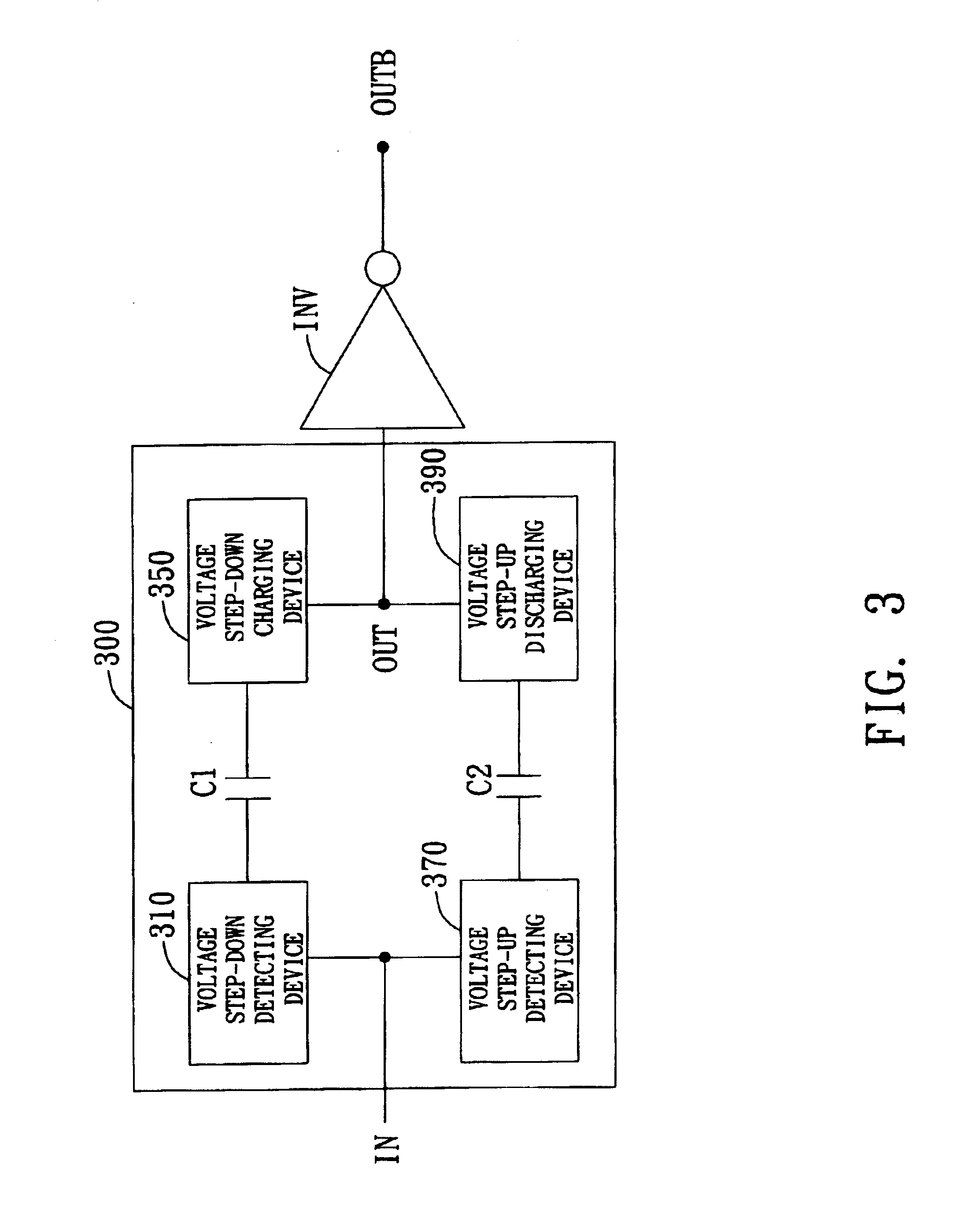
A high-threshold capacitor-coupling trigger 300 is illustrated in FIG. 3 according to a first embodiment of the invention in block diagram form. The high-threshold capacitor-coupling trigger (HCCT) 300 includes two capacitors C1, C2, a voltage step-down detecting device 310, a voltage step-down charging device 350, a voltage step-up detecting device 370, and a voltage step-up discharging device 390. The high-threshold capacitor-coupling trigger 300 has an output signal at the output terminal OUT and the output signal is a delayed version of an input signal IN. The voltage step-down detecting device 310 is used for detecting a slow decrease in the voltage of an input signal IN and outputting a step-down signal corresponding to and being delayed against the slow decrease during the slow increase. When the input signal IN decreases from a high level to a predetermined value, the voltage step-down detecting device 310 outputs the step-down signal corresponding to the dec...

Example

SECOND EMBODIMENT

A low-threshold capacitor-coupling trigger 500, as shown in FIG. 5, is a block diagram of a second embodiment of the invention, with an input terminal IN and an output terminal OUT. The low-threshold capacitor-coupling trigger 500 can be used as a signal receiver for signals from an interconnect line, for example. The low-threshold capacitor-coupling trigger 500 includes capacitors C1, C2, accelerating devices 555, 595, a voltage step-down detecting device 510, a voltage step-down charging device 550, a voltage step-up detecting device 570, and a voltage step-up discharging device 590. The voltage step-down detecting device 510, coupled to the input terminal IN, is used for detecting a slow voltage decrease of an input signal at the input terminal so as to output a step-down signal corresponding to the input signal. When the input signal drops from a high level, the voltage step-down detecting device 510 outputs the step-down signal according to the decrease of the ...

Example

As shown above, the main difference in implementation between the first and the second embodiments is the two positive feedback loops, including the accelerating devices 555 and 595 individually, for accelerating the response speed of the latter. In addition, the voltage step-down detecting devices in FIGS. 4A and 6A are different.

In the following, two operation modes of the low-threshold capacitor-coupling trigger 500 in FIG. 6A are described. In addition, the timing diagram of the signals involved in this circuit can be referred to FIG. 6B. In the initial state of the first operation, the voltage at the input terminal IN, the voltage of the inverted control signal CO1, the voltage at the output terminal OUT, and the voltage of the control signal CO2 are supposed to be VDD, VDD, ground, and ground respectively. When the input signal at the input terminal IN begins to fall at time t1 (as indicated in FIG. 6B), the voltage at node C, that is, the step-down signal, drops as well. By t...


PUM


Abstract

A capacitor-coupling acceleration apparatus is an accelerating circuit capable of being applied to interconnect lines in an integrated circuit in order to reduce delay owing to parasitic resistance and capacitance of the interconnect lines in the integrated circuit. The apparatus can be disposed between the interconnect lines. When a signal transmitted on the interconnect line has a change from a low-level voltage to a high-level voltage, the apparatus detects the voltage level change of the signal and provides a charging loop to charge the interconnect line, thereby accelerating the change from the low-level voltage to the high-level voltage. When a signal on the interconnect line has a change from the high-level voltage to the low-level voltage, the apparatus detects the voltage level change of the signal and provides a discharging loop to discharge the interconnect line, thereby accelerating the change from the high-level voltage to the low-level voltage.

Description

This application claims the benefit of Taiwan application Serial No. 091106057, filed Mar. 27, 2002.BACKGROUND OF THE INVENTION1. Field of the InventionThe invention relates in general to a capacitor-coupling device, and more particularly to a capacitor-coupling accelerator for use in an integrated circuit.2. Description of the Related ArtIn modem integrated circuit design, the delays of interconnect lines in a chip determine the performance of the whole chip. For the progress of the VLSI manufacturing process and the need for system-on-chip (SOC) integration, the gate delays in a chip are reduced when the devices in the chip are scaled down. Unfortunately, interconnect lines are lengthened along with the chip when the chip becomes larger. Besides, interconnect delays are made larger because greater RC effects result from the smaller line width of the interconnect lines and the narrower space between the interconnect lines. The performance of the whole chip would thus be degraded. A...

Claims


Application Information

Patent Timeline
IPC IPC(8): H03K19/017H03K19/01
CPCH03K19/01707
Inventor HUANG, HONG-YICHEN, SHIH-LUN
Owner IND TECH RES INST
Why Eureka
Try Eureka