Emission process for a single photon, corresponding semiconducting device and manufacturing process

a manufacturing process and single photon technology, applied in the field of single photon sources, can solve the problems of not being easily used reproduced, and achieve the effect of improving the probability of a single photon being emitted and improving electrical coupling

Inactive Publication Date: 2005-02-08
STMICROELECTRONICS SRL
View PDF4 Cites 0 Cited by
  • Summary
  • Abstract
  • Description
  • Claims
  • Application Information

AI Technical Summary

Benefits of technology

Advantageously, the device according to the invention may comprise several adjacent quantum boxes that can be arranged in the same horizontal plane and / or in adjacent stacked horizontal planes. The probability of a single photon being emitted is thus increased by the recombination of the single electron in one of the quantum boxes.
To achieve better electrical coupling between the drain region of the transistor and the quantum boxes, it is preferable if the substrate comprises an additional implanted region located under each quantum box, with the same type of conductivity as the drain region, and in contact with the drain region. For example, each quantum box may comprise germanium encapsulated in silicon.

Problems solved by technology

However, the oscillation phenomenon was the result of electrostatic disorders in the structure, and therefore, was not controlled and consequently could not be readily used reproduced.

Method used


Image

  • Emission process for a single photon, corresponding semiconducting device and manufacturing process
  • Emission process for a single photon, corresponding semiconducting device and manufacturing process
  • Emission process for a single photon, corresponding semiconducting device and manufacturing process

Examples


Embodiment Construction

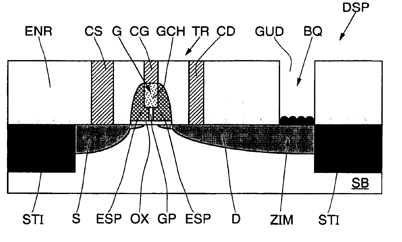
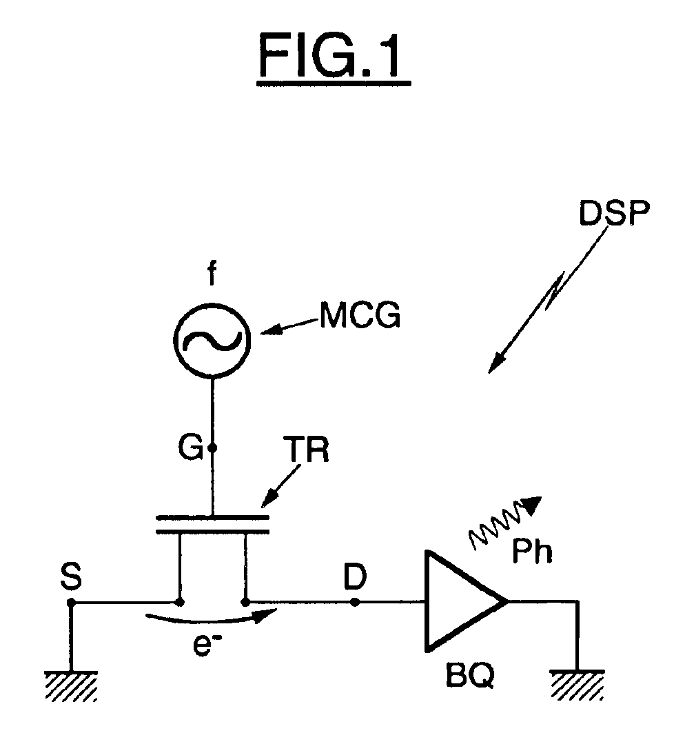
In FIG. 1, the DSP reference denotes a semiconductor device forming a single photon source. This device comprises a MOS transistor TR, the source of which is connected to ground, and is capable of outputting a single electron on its drain in response to a control voltage applied to its gate G. The control voltage is output by control means MCG. The control means MCG may also apply a voltage on the drain D.

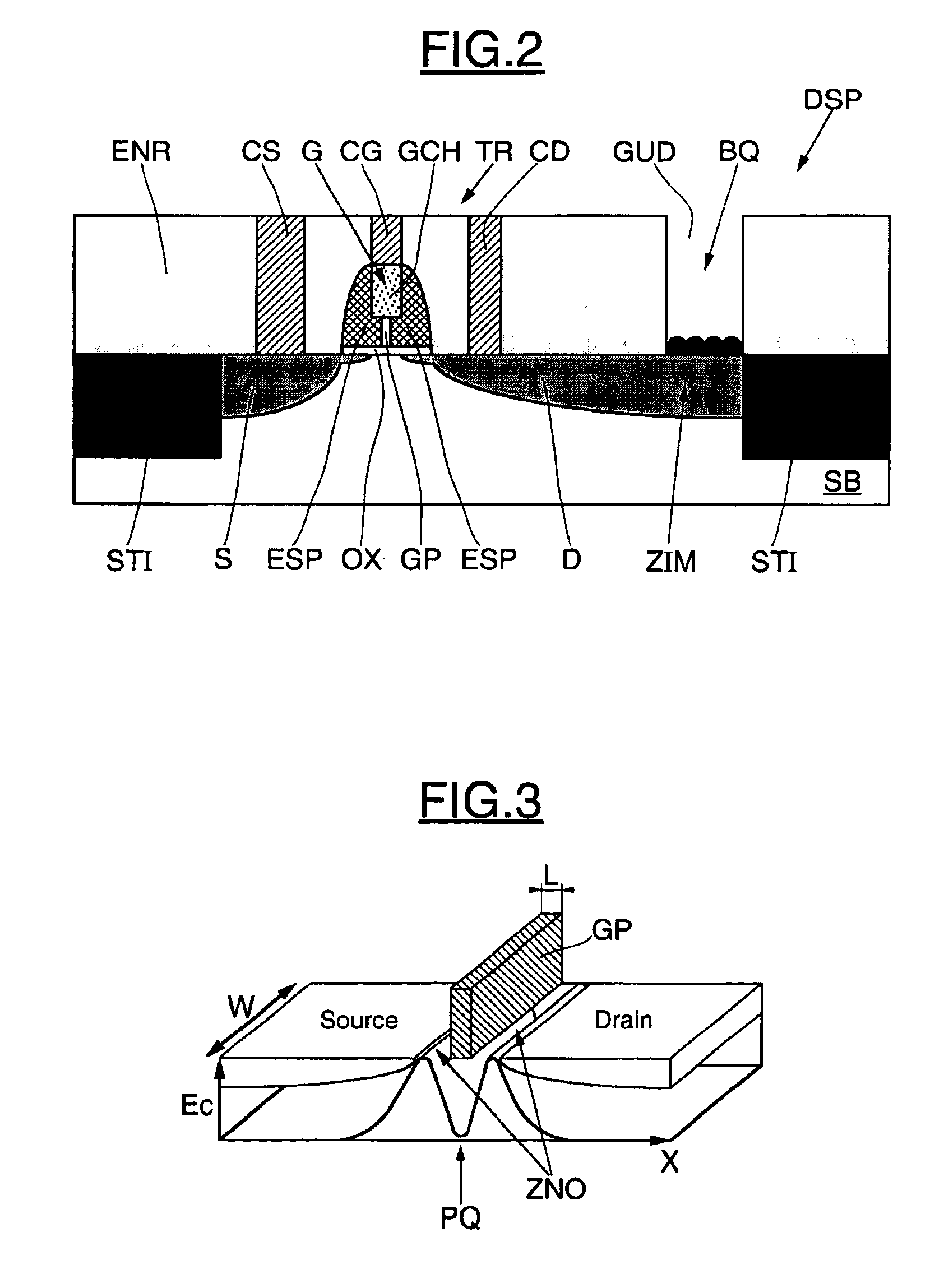
A quantum box BQ is connected to this drain, and the single electron emitted by the transistor will be trapped in this quantum box and will recombine for generating the emission of a single photon ph. As illustrated in FIGS. 2 and 3, this device DSP is made in integrated form on a semiconductor chip in which the substrate, which is P− doped for example, is referenced SB.

The transistor TR, for example an NMOS transistor, has a gate G in the shape of a mushroom or a T. More precisely, the gate G of the transistor comprises a gate bottom GP with a length L (the length is a distance me...


PUM


Abstract

An integrated circuit includes a semiconductor device forming a single photon source, and includes a MOS transistor on a silicon substrate. The MOS transistor has a mushroom shaped gate for outputting a single electron on its drain in a controlled manner in response to a control voltage applied to its gate. The transistor also includes at least one silicon compatible quantum box. The quantum box is electrically coupled to the drain region of the transistor, and is capable of outputting a single photon on reception of a single electron emitted by the transistor.

Description

FIELD OF THE INVENTIONThe present invention relates to integrated circuits, and more particularly, to single photon sources. The present invention is advantageously applicable to the field of cryptographic communications, for example.BACKGROUND OF THE INVENTIONThe current problem with cryptographic communications is due to the fact that the message transmitted from point A to point B can be copied in the interval that separates the two points. To overcome this problem, sources are used that emit only a single photon at a time to transmit binary random key type messages. An example of this type of use is described in the article by J. Rarity et al. entitled “Single Photon Sources And Applications”, Confined Photon System Fundamental And Applications, Springer Verlag LNP 351, pages 352-365.However, the remaining problem is to make such a source that emits only one photon at a time. At the present time, there are two major techniques. The first is based on extreme attenuation of a lase...

Claims


Application Information

Patent Timeline
Patent Type & Authority Patents(United States)
IPC IPC(8): H01S5/34H01S5/00
CPCB82Y20/00H01S5/341Y10S438/962H01S5/3412
Inventor MONFRAY, STEPHANEDUTARTRE, DIDIERBOEUF, FREDERIC
Owner STMICROELECTRONICS SRL
Why Eureka
Try Eureka