Substrate within a Ni/Au structure electroplated on electrical contact pads and method for fabricating the same

a technology of ni/au structure and substrate, which is applied in the direction of resist details, conductive pattern reinforcement, double resist layers, etc., can solve the problems of increasing fabrication costs, reducing circuit layout area and noise generated at high frequency, and reducing the effect of circuit layout pattern effective area and noise reduction

Inactive Publication Date: 2005-02-08
PHOENIX PRECISION TECH CORP
View PDF5 Cites 15 Cited by
  • Summary
  • Abstract
  • Description
  • Claims
  • Application Information

AI Technical Summary

Benefits of technology

The major object of the present invention is to provide a method for fabricating a substrate within a Ni / Au structure electroplated on electrical contact pads. In this method, the conducting wires for electroplating are not necessary to be formed on the substrate, so that the effective area for circuit layout pattern is increased and the noise is thus reduced.

Problems solved by technology

To catch the downsize trend of the electronics technology development, some issues have impacted the progress of substrates for integrated circuits (IC) packaged.
In addition, noise due to the antenna effect when the conducting wires are employed may occur at high frequency.
Unfortunately, It still exists some defects in this issue such as reduced circuit layout area and noise generated at high frequency.
Even though the conducting wires for electroplating the Ni / Au layer are not required in this case, the circuit layout pattern 25 (including electrical contact pads 26 and the electrically conducting traces) on each surface of the substrate 2 are coated with a Ni / Au layer, resulting in increasing fabrication cost since metal Ni / Au is very expensive.
The exposed portions are corrosion due to oxidation, and the adhesion of bonding pads will be weak for lack of coverage with gold.
Therefore, during the bonding process, electrodes on the chip and bonding pads on the substrate are bonded together by gold wires (not shown), the electrical coupling between gold wires and the bonding pads may be negative affected.
Furthermore, the Ni / Au 23 on the circuit layout pattern 25 covered by the solder mask 27 (Illustrated as FIG. 2E) to prevent soldering on the top surface of the substrate 2 does not have reliable coupling due to lower adhesion between different materials resulting in poor yield.

Method used


Image

  • Substrate within a Ni/Au structure electroplated on electrical contact pads and method for fabricating the same
  • Substrate within a Ni/Au structure electroplated on electrical contact pads and method for fabricating the same
  • Substrate within a Ni/Au structure electroplated on electrical contact pads and method for fabricating the same

Examples


Embodiment Construction

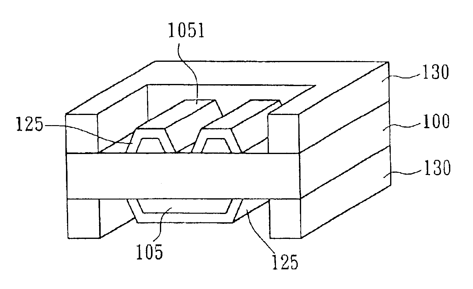
The present invention providing a substrate within a Ni / Au structure electroplated on electrical contact pads and a method for fabricating the same can be described hereinafter by the preferred embodiment. FIG. 3A to FIG. 3H show the fabrication process of a Ni / Au structure electroplated on electrical contact pads of a substrate according to the preferred embodiment of the present invention.

Illustrated as FIG. 3A, providing a substrate 100 with plated through holes or blind vias. Then, a circuit layout pattern 105 is formed by photolithography and etching process.

Illustrated as FIG. 3B, a conducting film 110 is composed of one of Sn, Cu, Cr, Pd, Ni, Sn / Pb and combination formed on the substrate 100 to be the conducting circuits for electroplating. Wherein the materials for forming the conducting film 110 are examples, don't limited to the foregoing materials in any practical application. By means of any electrically conducting metal formed within one of sputtering, electroless plati...


PUM


Abstract

The present invention discloses a substrate within a Ni/Au structure electroplated on electrical contact pads and a method for fabricating the same. The method comprises: providing a substrate with a circuit layout pattern and forming a conducting film on the surface of the substrate; depositing a first photoresist layer within an opening on said electrical conducting film surface to expose a portion of said circuit layout pattern to be electrical contact pads; removing the exposed conducting film uncovered by the first photoresist layer; depositing a second photoresist layer, covering the conducting film exposed in the openings of the first photoresist layer; electroplating Ni/Au covering the surface of the electrical contact pads; removing the first and second photoresists, and the conducting film covered by the photoresists; depositing solder mask on the substrate within an opening to expose said electrical contact pads. It improves the electrical coupling between gold wires and the electrical contact pads of the substrate, prevents the electrical contact pads from oxidation, and insurances the electrical interconnection performance.

Description

BACKGROUND OF THE INVENTION1. Field of the InventionThe present invention relates to a substrate within a Ni / Au structure electroplated on the electrical contact pads and a method for fabricating the same.2. Description of the Prior ArtTo catch the downsize trend of the electronics technology development, some issues have impacted the progress of substrates for integrated circuits (IC) packaged. On the surface of the substrate, electrical contact pads connected to a plurality of conducting wires is formed for the transmission of electronic signals or power. On the top surface of the electrical contact pads, a metal Ni / Au layer is formed. Some electrical contact pads, also known as bonding pads, of a substrate are covered with a Ni / Au layer on the surface. During the wire-bonding process, the metal wires and the bonding pads are all made of gold, resulting in excellent electrical coupling. Furthermore, other electrical contact pads of a substrate, solder ball pads for example, are co...

Claims


Application Information

Patent Timeline
Patent Type & Authority Patents(United States)
IPC IPC(8): H01L21/02H01L23/48H01L23/498H01L21/48H05K3/24
CPCH01L21/4846H01L23/49811H05K3/243H05K2203/0542H05K2203/0577H01L2924/0002H05K2203/1476H01L2924/00
Inventor HSU, SHIH-PINGCHEN, CHIANG-DULIU, YEN-HUNG
Owner PHOENIX PRECISION TECH CORP
Why Eureka
Try Eureka