

Electron-emitting device, electron source, image forming apparatus, and electron-emitting apparatus
- Summary
- Abstract
- Description
- Claims
- Application Information
AI Technical Summary
Benefits of technology
Problems solved by technology
Method used
Image

Examples
seventh embodiment
[0038]FIG. 14 is a schematic cross-sectional view of an electron-emitting device ;
[0039]FIG. 15 is a schematic plain view of the electron-emitting device according to the seventh embodiment;
[0040]FIG. 16 is a schematic cross-sectional view of a diode type electron-emitting device among FE type electron-emitting devices;
[0041]FIG. 17 is a schematic cross-sectional view of an edge emitter type electron-emitting device among the FE type electron-emitting devices;
[0042]FIGS. 18A and 18B are schematic cross-sectional views used to explain the construction of the electron-emitting device of the present invention;
[0043]FIG. 19 is a schematic diagram illustrating a construction of a fiber whose main ingredient is carbon; and
[0044]FIG. 20 is a schematic diagram illustrating another construction of the fiber whose main ingredient is carbon.
DETAILED DESCRIPTION OF THE PREFERRED EMBODIMENTS
[0045]The preferred embodiment of the present invention will be exemplarily described in detail below with...
first embodiment
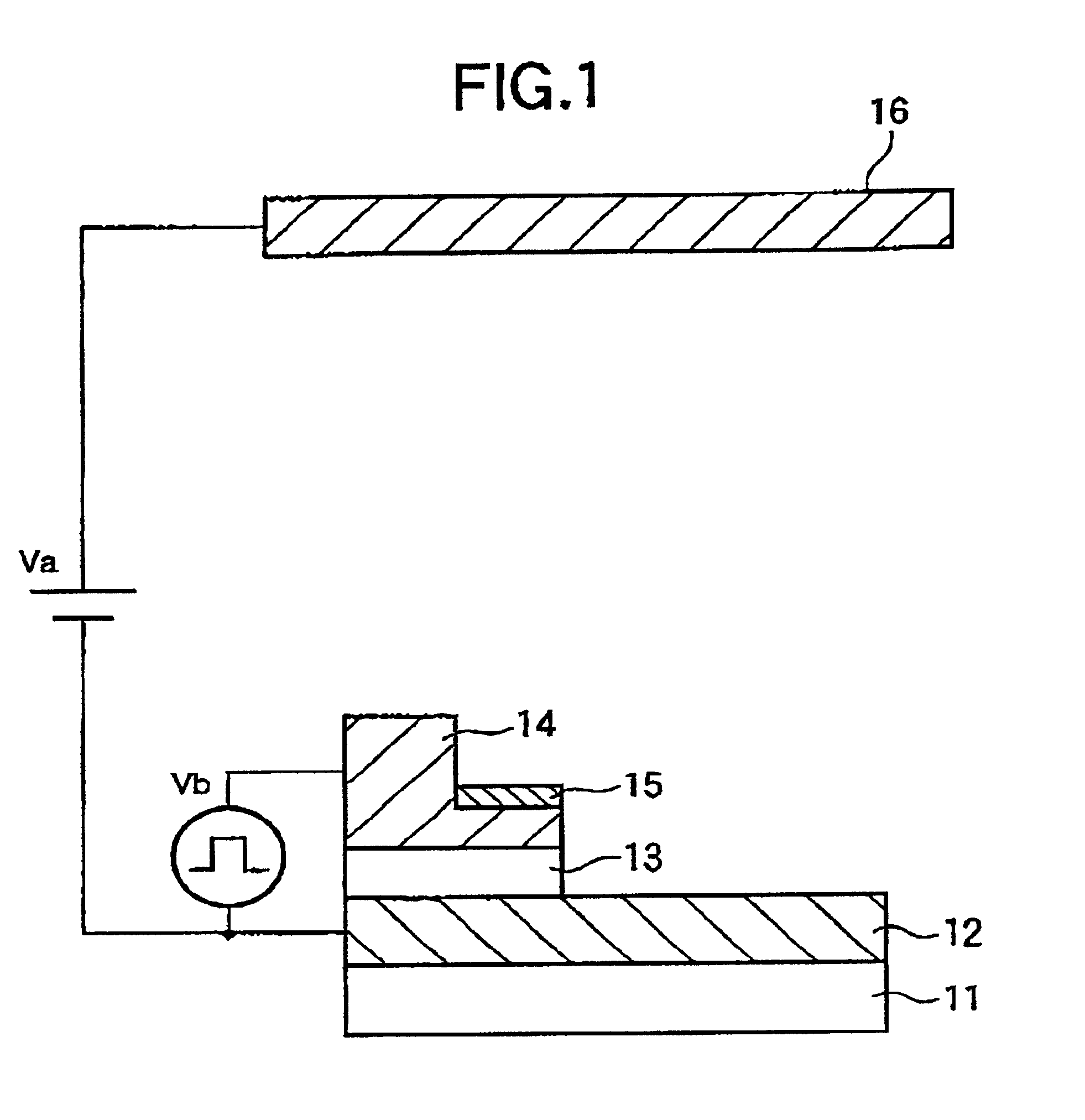
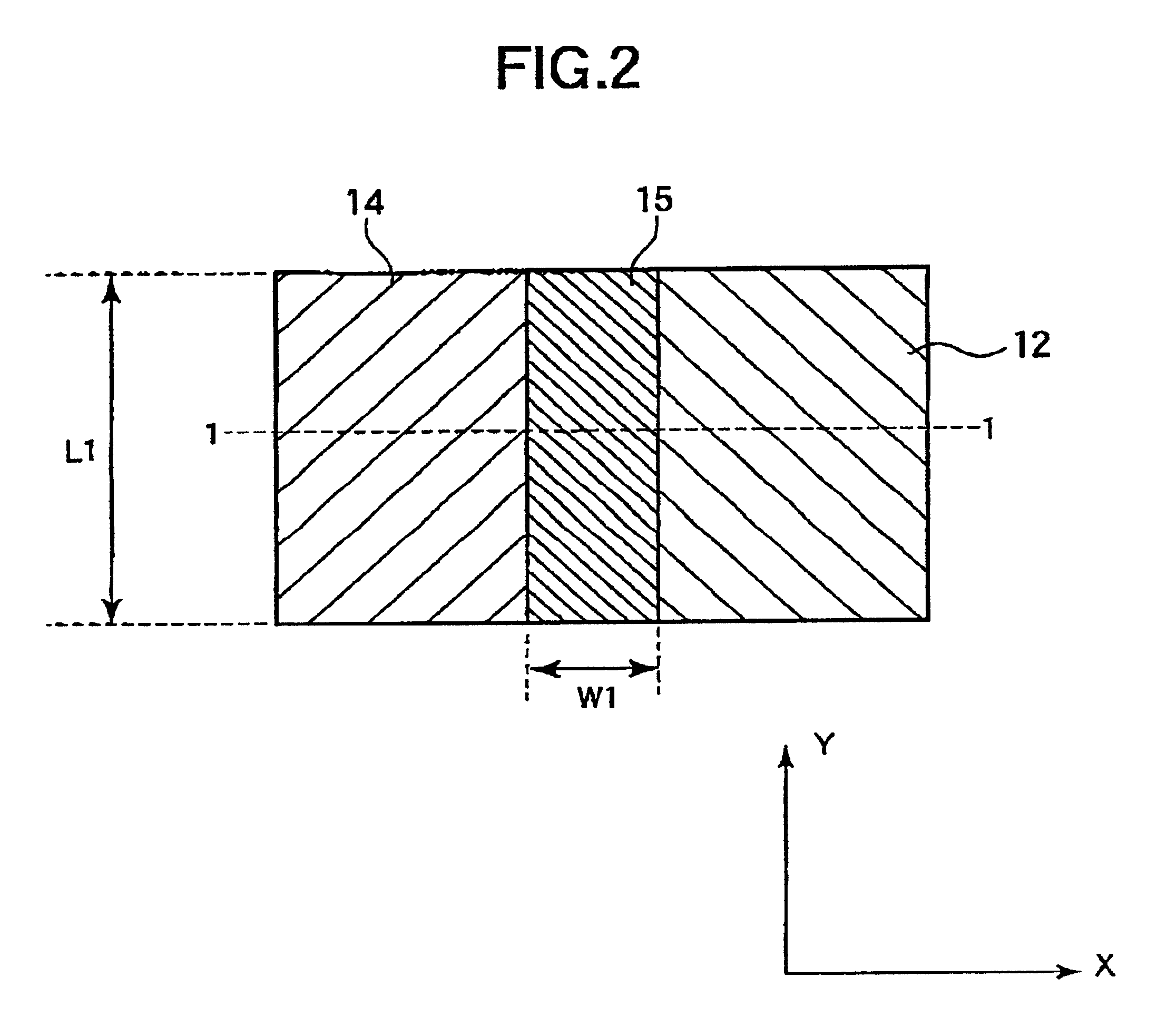
[0107]FIG. 2 is a plan view of the electron-emitting apparatus of the FIG. 1 is a cross sectional view of the electron-emitting apparatus, and FIGS. 5A to 5G show a method of manufacturing the electron-emitting apparatus. The method of manufacturing the electron-emitting apparatus of this embodiment is described in detail below.
[0108](Step 1)
[0109]Firsts as shown in FIG. 5A, with a sputtering method, the first electrode 12 that is an Al film having a thickness of 300 nm, the insulating layer 13 that is an SiO2 film having a thickness of 100 nm, and the second electrode 14 that is a Ta film having a thickness of 400 nm are stacked in this order on the substrate 11 that is a sufficiently cleaned quartz glass.
[0110](Step 2)
[0111]Next, as shown in FIG. 5B, a photomask pattern of a positive photoresist (AZ1500 manufactured by Clariant) is formed by spin coating, and is exposed to light and developed with a photolithography method to obtain a mask pattern 18. Then, as shown in FIG. 5C, d...
third embodiment
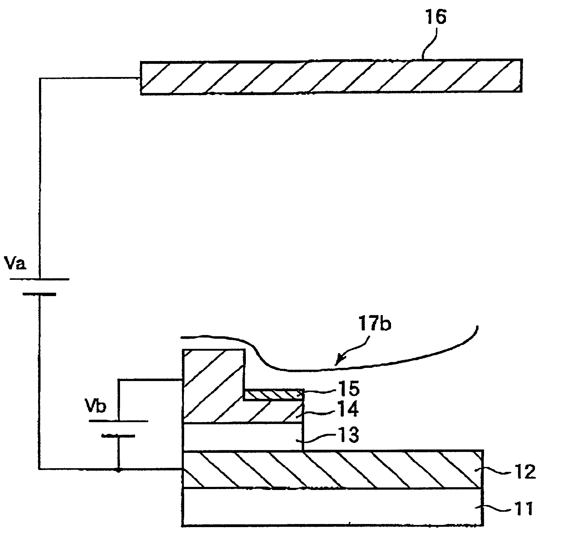
[0126]A schematic cross-sectional view of the electron-emitting device manufactured in the third embodiment is shown in FIG. 1. In this embodiment, the applied voltage Va is increased so as to improve the current amounts of emitted electrons. The following description centers on the characteristic points of this embodiment and therefore the same points as in the aforementioned embodiments are omitted.
[0127]In this embodiment, the voltage Va applied to drive the electron-emitting device of the first embodiment is set at 15 kV and the distance D1 between the electron-emitting film 15 and the anode 16 is set at 2 mm.
[0128]The electron-emitting device performs electron emission by means of the electric field formed by the anode voltage, so that the increased anode voltage improves the current amounts of the emitted electrons in this embodiment At the same time, however, the area from which electrons are emitted is also extended and therefore the beam diameter of the emitted electrons is...
PUM
 Abstract
Description
Claims
Application Information