Electrooptical device, method of manufacturing the same, and electronic equipment

a technology of optical shutter and optical axis, applied in the direction of optics, instruments, electrical equipment, etc., can solve the problems of poor display, loss of function as a normal optical shutter, poor rubbing, etc., to prevent the occurrence of disclination, reduce the area of a required black mask, and increase the effect of effective pixel area

Inactive Publication Date: 2005-02-15
SEMICON ENERGY LAB CO LTD
View PDF127 Cites 82 Cited by
  • Summary
  • Abstract
  • Description
  • Claims
  • Application Information

AI Technical Summary

Benefits of technology

The present invention has been made in view of the foregoing problems, and provides a technique relating to the structure of a contact portion to form a completely flat conductive layer. Particularly, an object of the present invention is to completely flatten a pixel electrode of an AMLCD and to prevent the occurrence of disclination caused from a difference in level at a contact portion. Then the area of a required black mask is decreased, so that an effective pixel area is enlarged and an AMLCD with high fineness and high contrast is realized.

Problems solved by technology

Although the liquid crystal is arranged between the pixel electrode and the opposite electrode, with orientation having some regularity, there is a case where the orientation is disturbed by poor rubbing due to the asperities of the surface of the electrode.
In this case, the function as a normal optical shutter is lost at that portion, and poor display, such as light leak, is caused.
Conventionally, although means, such as a structure of covering a TFT with a flattened film, have been contrived to prevent the disclination, the means do not necessarily become fundamental solutions.
This is because even if a flattened film is used, it is impossible to flatten a difference in level at a contact portion of a finally formed pixel electrode.

Method used


Image

  • Electrooptical device, method of manufacturing the same, and electronic equipment
  • Electrooptical device, method of manufacturing the same, and electronic equipment
  • Electrooptical device, method of manufacturing the same, and electronic equipment

Examples


embodiment 1

[Embodiment 1]

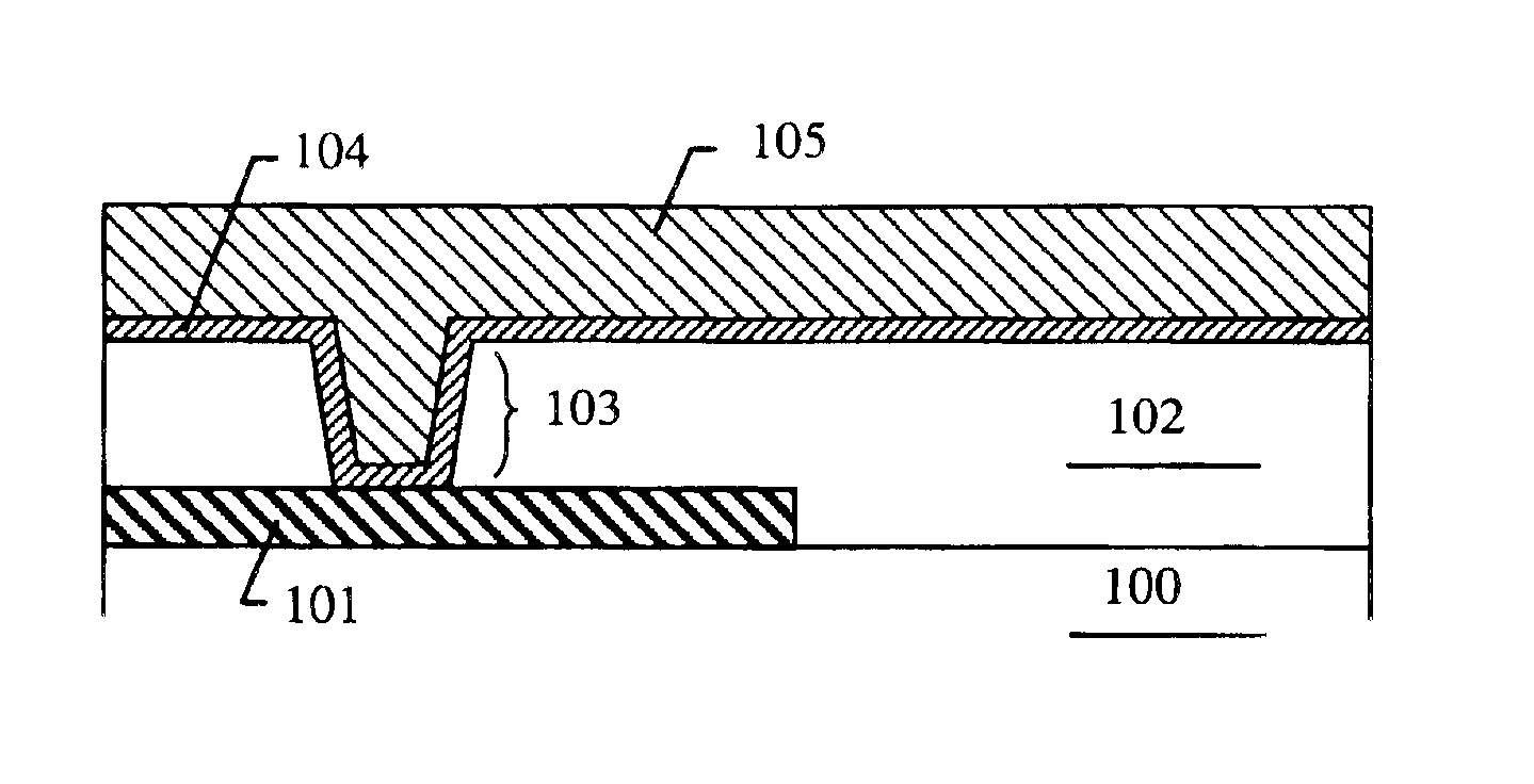
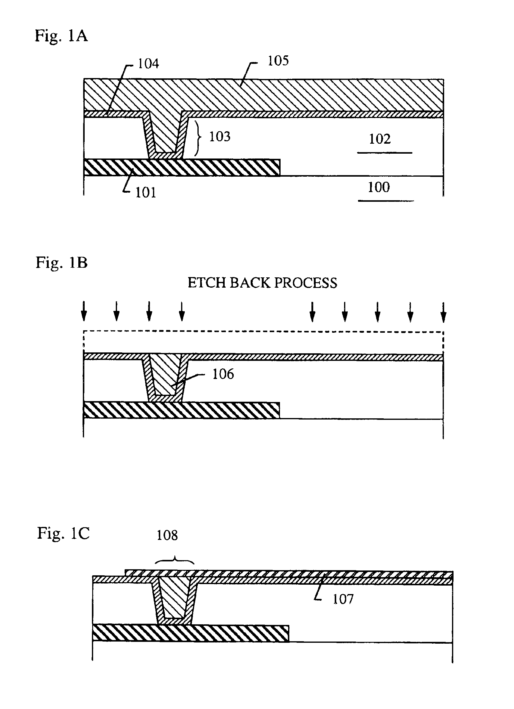
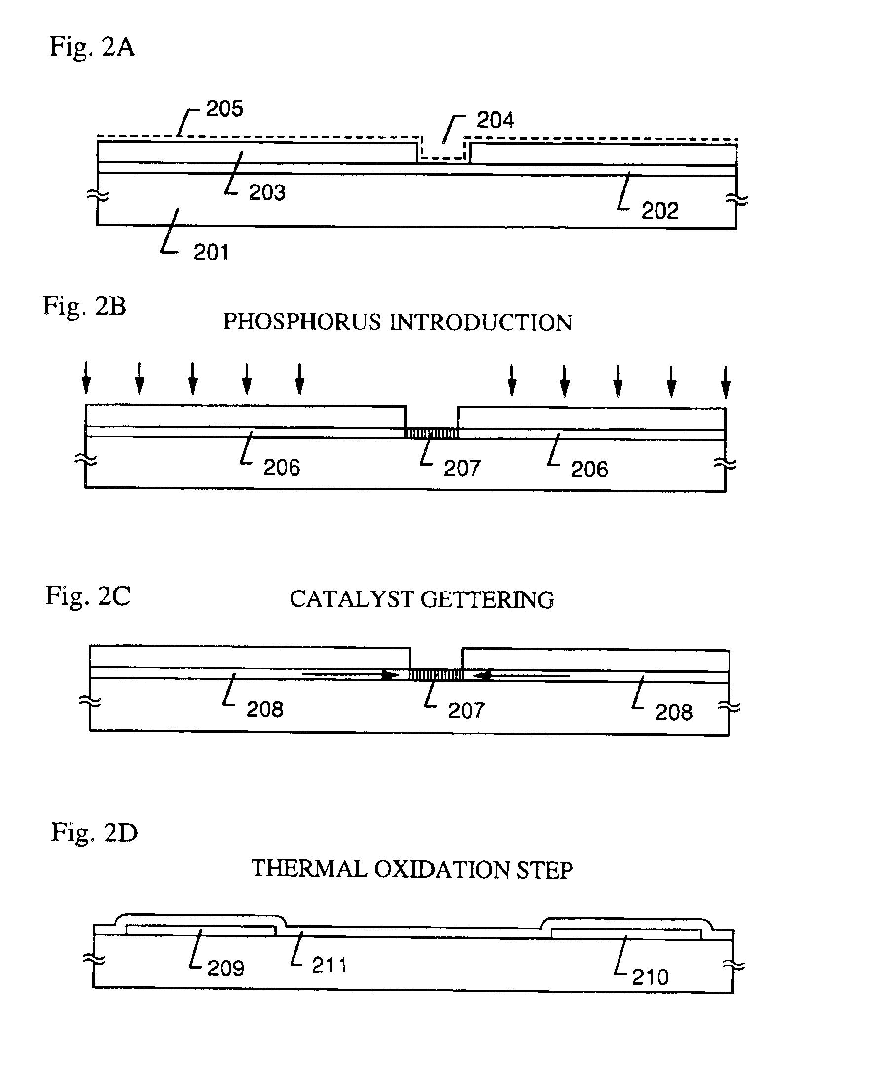
In this embodiment, a method of manufacturing a unit pixel (unit picture element) constituting a pixel matrix circuit of an active matrix type liquid crystal display device driven in a reflection mode will be described with reference to FIGS. 2A to 2D.

First, a quartz substrate 201 as a substrate having an insulating surface is prepared. In this embodiment, since a heat treatment at 900 to 1100° C. is carried out later, it is necessary to use a material having high heat resistance. Other than the quartz substrate, a crystallized glass (glass ceramic) substrate provided with an under film, a silicon substrate provided with a thermal oxidation film, or the like may be used.

An amorphous silicon film 202 with a thickness of 65 nm is formed thereon, and the amorphous silicon film 202 is crystallized by using a technique disclosed in Japanese Patent Unexamined Publication No. Hei. 8-78329. The technique of the publication is the one for carrying out selective crystallization ...

embodiment 2

[Embodiment 2]

In the embodiment 1, although the etch back treatment is carried out to the embedded conductive layer so that filling of the opening portion is carried out, it is also possible to carry out a polishing treatment instead of the etch back treatment. Typically, it is also by possible to adopt a technique called CMP (Chemical Mechanical Polishing).

In the case where this technique is used, although it is necessary to pay attention to the occurrence of dust, if this technique is used, there is no fear of excess overetching in the opening portion. Moreover, since to the first metal layer can function as a polishing stopper, excellent flatness can be realized.

embodiment 3

[Embodiment 3]

In this embodiment, a technique for manufacturing a reflection type AMLCD by a structure different from the embodiment 1 will be described with reference to FIGS. 5A to 5C.

First, in accordance with the manufacturing steps of the embodiment 1, a third interlayer insulating film 237 is formed, and an opening portion 501 is formed. Then a pixel electrode 502 is formed so as to cover the third interlayer insulating film 237 and the opening portion 501 (FIG. 5A).

Next, an embedded insulating layer 502 having a thickness of 2 μm is formed so as to cover the pixel electrode 502. In this embodiment, a polyimide resin film is used as the embedded insulating layer (FIG. 5B).

Next, the embedded insulating layer 503 is made to retreat (the thickness is made thin), so that an embedded insulating layer 504 is formed in a recess portion formed on the pixel electrode 502 through the opening portion 501. At the same time, an embedded insulating layer 505 is formed in a gap between adjace...


PUM

PropertyMeasurementUnit
heat resistanceaaaaaaaaaa
thicknessaaaaaaaaaa
thicknessaaaaaaaaaa

Abstract

An AMLCD having high fineness and high contrast is realized. First, an interlayer film is provided on an element electrode, and an opening portion is formed in the interlayer film. Next, after a first metal layer is formed, an embedded insulating layer is formed. The embedded insulating layer is retreated by a means, such as an etch back method, to realize a state in which only the opening portion is filled with the embedded insulating layer. By this, electric connection between the element electrode and a second metal layer becomes possible while keeping the flatness.

Description

BACKGROUND OF THE INVENTION1. Field of the InventionThe present invention relates to an electrooptical device (particularly, a reflection type liquid crystal display device), and more particularly to a structure of each of a plurality of pixel electrodes provided in a pixel matrix circuit in the electrooptical device.2. Description of the Related ArtIn recent years, a technique for manufacturing a TFT on an inexpensive glass substrate has been rapidly developed. The reason is that the demand for an AMLCD (Active Matrix Liquid Crystal Display) has been increased.In the AMLCD, a thin film transistor (TFT) as a switching element is disposed for each of several tens to several millions of pixels arranged in matrix, and an electric charge going in and out of each of pixel electrodes is controlled by a switching function of the TFT.A liquid crystal is put between the respective pixel electrodes and an opposite electrode, and a kind of capacitor is formed. Thus, if an electric charge going...

Claims


Application Information

Patent Timeline
Patent Type & Authority Patents(United States)
IPC IPC(8): G02F1/1335G02F1/13G02F1/1362G02F1/1333G02F1/136G02F1/1368H01L21/336H01L29/786
CPCG02F1/133553G02F1/136227G02F2001/133357G02F1/133357
Inventor HIGUCHI, MASAYUKIMURAKAMI, SATOSHINAKAZAWA, MISAKO
Owner SEMICON ENERGY LAB CO LTD
Why Eureka
Try Eureka