

Vacuum-processing method using a movable cooling plate during processing
- Summary
- Abstract
- Description
- Claims
- Application Information
AI Technical Summary
Benefits of technology
Problems solved by technology
Method used
Image

Examples
example 1
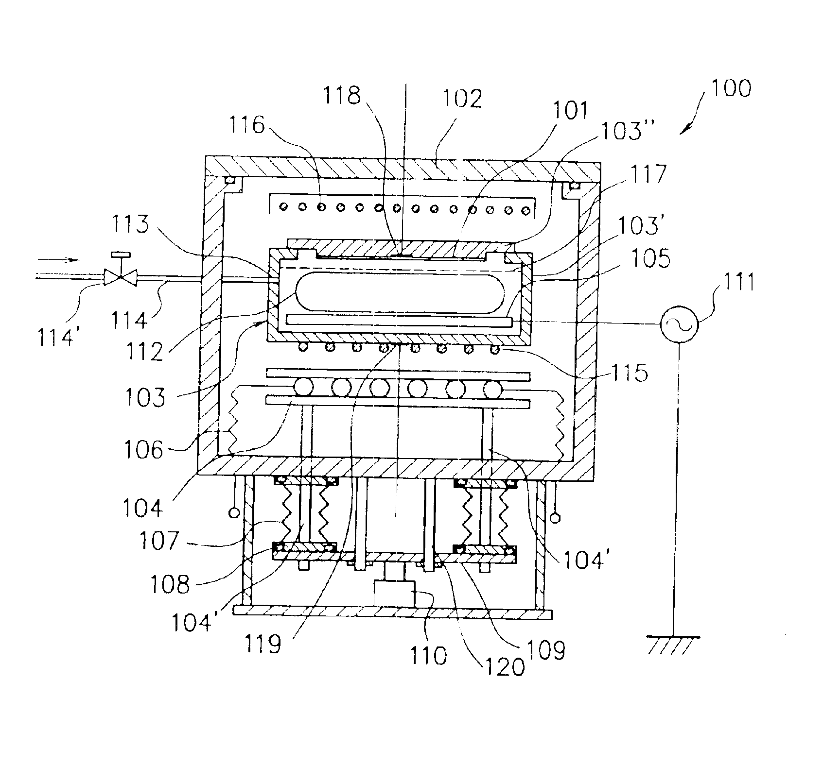
FIG. 1 is a schematic diagram illustrating an example of a vacuum-processing apparatus of the present invention. In FIG. 1, reference numeral 100 indicates a vacuum-processing apparatus. As shown in FIG. 1, the vacuum-processing apparatus 100 has a vacuum vessel 102 whose inside is capable of being evacuated to be a reduced pressure state. In the inside of the vacuum vessel 102, there is provided a vacuum-processing chamber 103 constituted by a circumferential wall 103′ having a substrate-retaining member 103″ which is detachably joined with said circumferential wall 103′. Reference numeral 101 indicates a substrate arranged on the substrate-retaining member 103″ so as to downward face the inside of the vacuum-processing chamber 103. The vacuum-processing chamber 103 is used for vacuum-processing the substrate 101 arranged on the substrate-retaining member 103″ of the circumferential wall 103′.
The vacuum-processing for the substrate 101 include deposition treatment of a deposited fi...
example 2
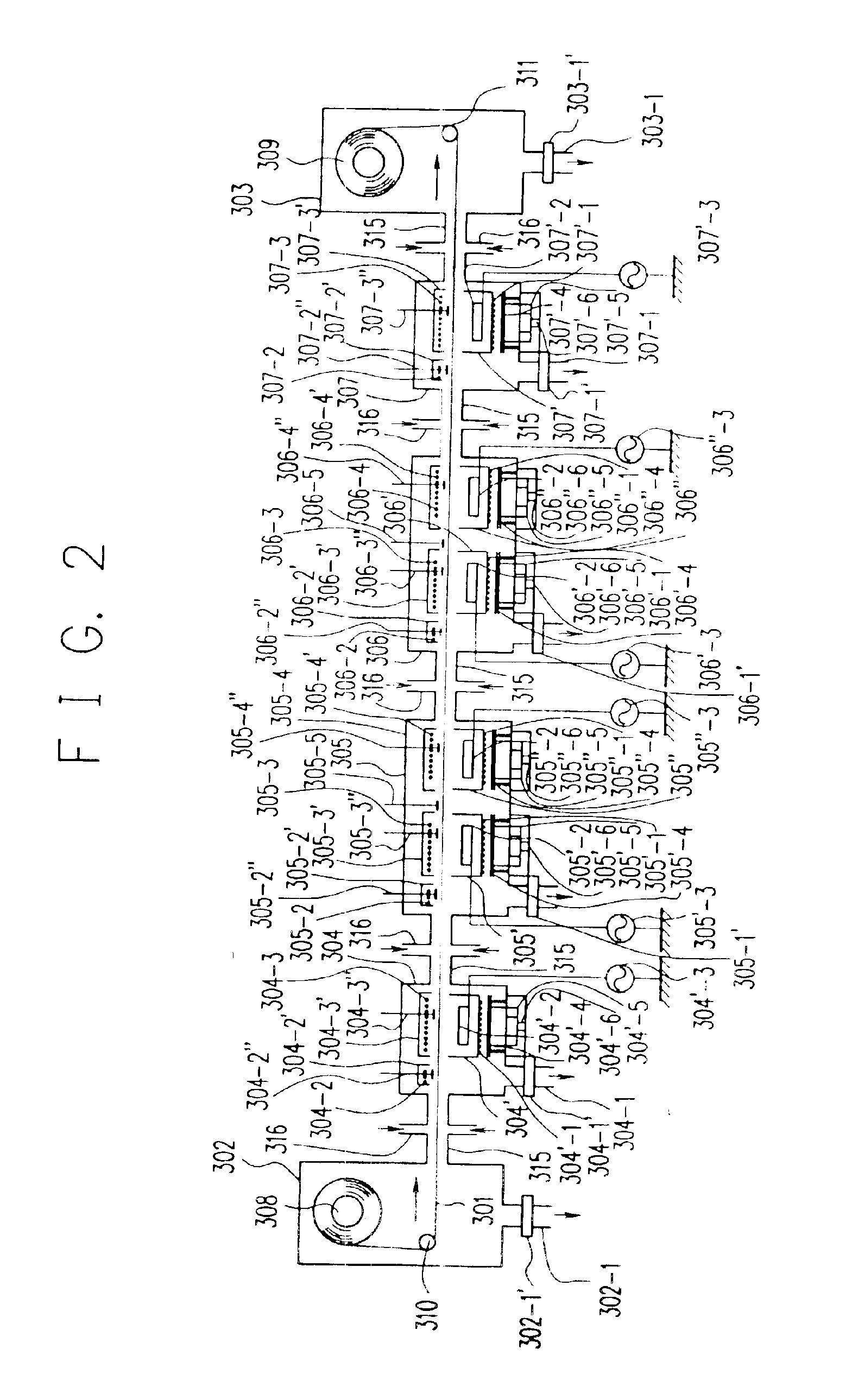
FIG. 2 is a schematic diagram illustrating an example of a vacuum-processing apparatus of the present invention. In FIG. 2, reference numeral 301 indicates a web substrate, and reference numeral 302 a substrate delivery vacuum vessel in which a pay-out bobbin 308 having the web substrate 301 wound thereon in a coil form is installed. The substrate delivery vacuum vessel 302 is provided with an exhaust pipe 302-1 provided with a throttle valve 302-1′ and which is connected to a vacuum pump (not shown). Reference numeral 303 indicates a substrate take-up vacuum vessel in which a take-up bobbin 309 for taking up the web substrate 301 thereon while being wound thereon in a coil form is installed. The substrate take-up vacuum vessel 303 is provided with an exhaust pipe 303-1 provided with a throttle valve 303-1′ and which is connected to a vacuum pump (not shown).
Reference numeral 304 indicates a first vacuum vessel provided with an exhaust pipe 304-1 provided with a throttle valve 304-1...
example 3
The solar cell-preparing procedures of Example 1 were repeated, except that the position of the cooling plate (306′-4, 306″-4) in the H2-plasma treating vacuum vessel 306 was changed with time elapse of the H2-plasma treatment by the vacuum-processing chamber (306′, 306″) as will be described below, to obtain 8 solar cell sample groups each comprising 20 solar cell samples (the 8 solar cell sample groups will be hereinafter referred to as Sample Ex.3-1 to Sample Ex.3-8).
In this example, the cooling plate (306′-4, 306″-4) in the H2-plasma treating vacuum vessel 306 was made to come closer to the circumferential wall of vacuum-processing chamber (306′, 306″) with time elapse of the H2-plasma treatment by the vacuum-processing chamber (306′, 306″) so that the temperature of the circumferential wall of vacuum-processing chamber (306′, 306″) became constant. Specifically, by actuating the fluctuation mechanism member (306′-5, 306″-5), the interval (the distance) between the cooling plate...
PUM
| Property | Measurement | Unit |
|---|---|---|
| Temperature | aaaaa | aaaaa |
| Temperature | aaaaa | aaaaa |
| Temperature | aaaaa | aaaaa |
Abstract
Description
Claims
Application Information