Electrooptical displays with polymer localized in vicinities of substrate spacers

a technology of electronic display and polymer, applied in the field of liquid crystal and other electronic displays, can solve the problems of high drive voltage, damage to the display within the device, repair and product return, etc., and achieve the effects of good performance, peeling strength, and optimizing the laminate structure of the plastic display

Inactive Publication Date: 2005-02-22
SAMSUNG DISPLAY CO LTD
View PDF30 Cites 4 Cited by
  • Summary
  • Abstract
  • Description
  • Claims
  • Application Information

AI Technical Summary

Benefits of technology

The invention provides displays that are simple, manufacturable, and that are capable of achieving polymer microstructures that are self-aligned (i.e., no photomask required) and localized to within less than about 5 μm. Additional benefits include the adhesion to the substrates of the spacing elements used to maintain the proper distance between the substrates. This is important since millions of these microscopic spacers may be distributed between the substrates of any of the aforementioned display technologies, and the spacers will have a tendency to shift upon flexure of the display or when the display is squeezed. Other benefits include the ability to optimize the laminate structure of the plastic display to provide good performance under compression as well as peel strength. This last benefit is achieved as a result of the polymer being localized around and surrounding the spacers; the spacers provide compressive strength while the polymer provides the peel and shear strength.

Problems solved by technology

In the area of mobile electronics, such as cell phones and personal digital assistants (PDAs), size and weight are critical factors to the commercial success of a product, but currently breakage of the displays within these devices remains the primary cause of repairs and product returns.
In all three of these cases, while they have some positive features such as high contrast and compatibility with plastic substrates, they all currently high drive voltages, have slow response times, and are not compatible with commercially available drive electronics.
Like the other flexible displays, PDLCDs required high drive voltages not generally compatible with existing drive electronics.
U.S. Pat. No. 5,949,508 describes a method in which a lamellar structure is achieved whereby the LC and polymer are disposed on opposite substrates; this reduces the drive voltages necessary to switch the device, but results in a structure where it is only practical to have the rubbed alignment surface on one of the substrates.
While this structure is effective with nematic or electrically controlled birefringence (ECB) displays, it becomes more difficult to construct displays such as twisted nematic (TN) and super twisted nematic (STN) which typically require alignment surfaces on both substrates.
Polymer structures of a size on the order of a pixel (˜0.3 mm) are achievable, but manufacturing may be more difficult since the photomask must generally be aligned to the electrode structure within the device and expensive collimated UV light sources must generally be employed.
Structures much smaller than 0.3 mm may be difficult to achieve due to the inherent scattering of the LC / polymer mixture.
Proper alignment of the silk-screening mask to the clear ITO electrodes may be difficult to achieve, and the introduction of chemicals directly onto the polyimide alignment surface may result in poor alignment of the LC to the alignment surface, poor appearance of the display and lower manufacturing yields.
In addition to the breakage problems due to shock and drop, glass substrate displays also have difficulty surviving extremes of temperature.
While the voids are small in size, they typically are noticeable enough that the display will be returned for repair.
As the display is cooled down, both the LC and spacer material will contract but due to the mismatch in the thermal coefficients of expansion and the mechanical discontinuity at the spacers, stress is localized around the spacers and voids develop.
Because of the difficulty of manufacturing these spacers, they are often 10-20 times more expensive than regular spacers and so are often used only when absolutely necessary.

Method used


Image

  • Electrooptical displays with polymer localized in vicinities of substrate spacers
  • Electrooptical displays with polymer localized in vicinities of substrate spacers
  • Electrooptical displays with polymer localized in vicinities of substrate spacers

Examples


Embodiment Construction

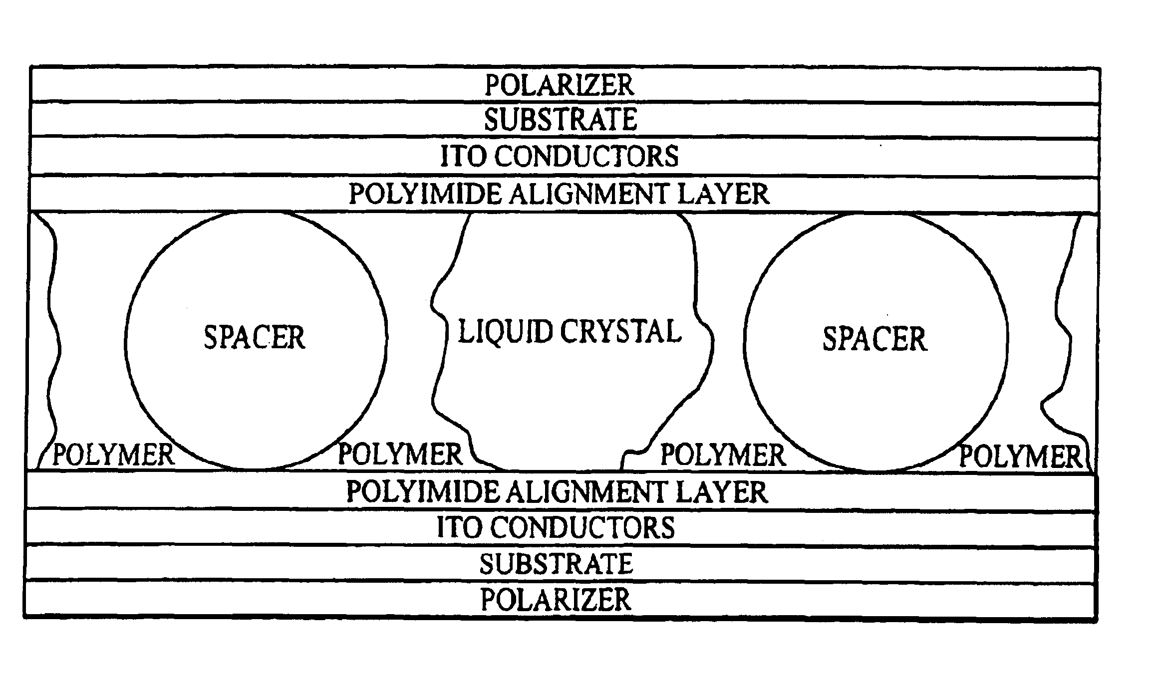
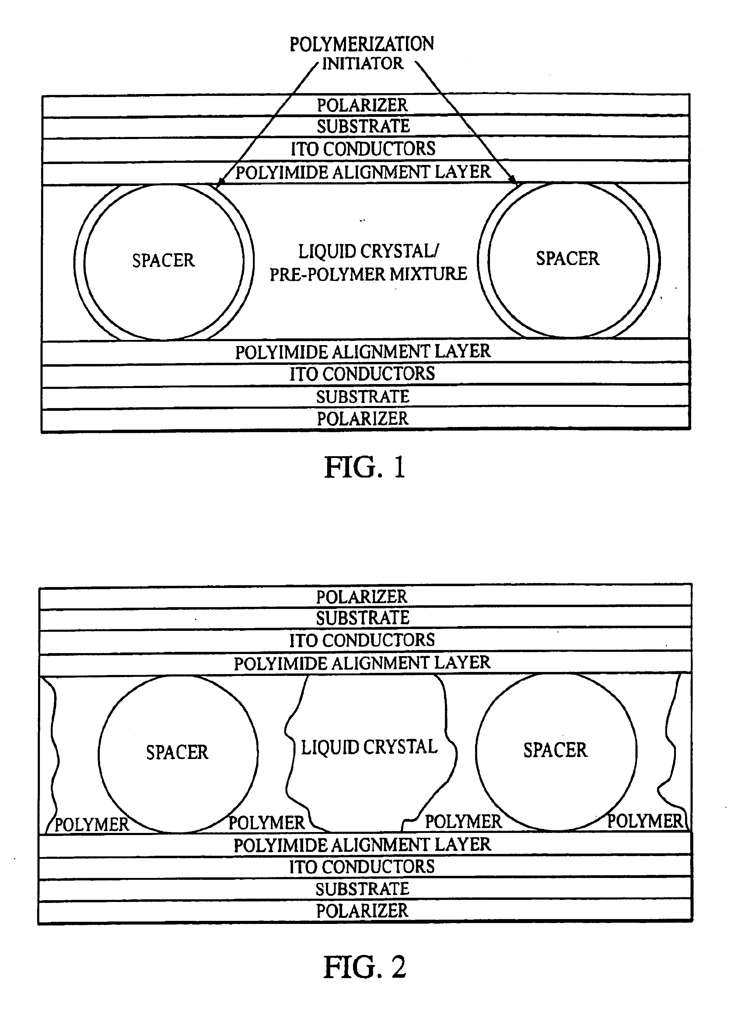
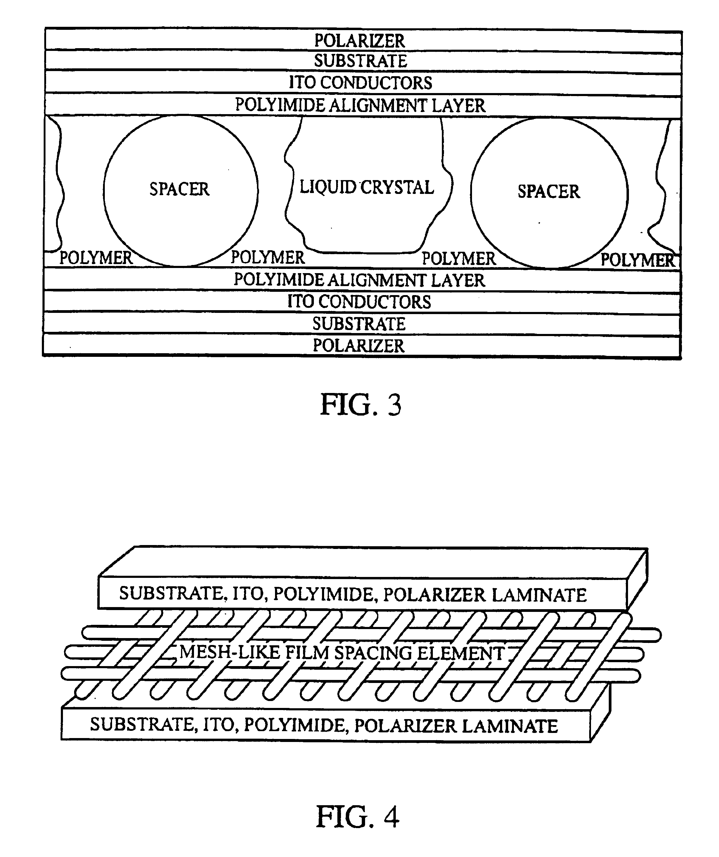
According to the present invention, in the preferred embodiment, a liquid crystal display device is assembled using the following procedure:1. The substrates are a flexible polymer material with a low level of birefringence to improve the optical qualities of the final product and having a glass transition temperature greater than 150 degrees C. in order to facilitate the various drying and baking operations. A polymer that meets these requirements is poly ether sulphone (PES). A vapor barrier is coated onto the outside surface of the substrate to improve the reliability and product life of the display; the vapor barrier is typically composed of a thin film laminate structure of silicon oxide and another polymer.2. The substrates are coated with a vacuum-deposited layer of typically indium tin oxide (ITO), which is a transparent conductor. The ITO is then patterned via chemical, electron beam, or laser etching.3. A mixture is prepared of approximately 10% photoinitiated pre-polymer ...


PUM

PropertyMeasurementUnit
sizeaaaaaaaaaa
diameteraaaaaaaaaa
wavelengthaaaaaaaaaa

Abstract

There is a liquid crystal display device with two substrates facing and spaced from each other, at least one of the substrates being transparent. Electrodes are positioned to establish an electric field in the space between the two substrates. One or more space elements are located between the substrates. One or more polymer supports are located primarily in the vicinities of the spacer elements. The polymer supports extend between the two substrates and have been polymerized in situ in response to polymerization initiating or enhancing (PIE) material carried on or within the spacer elements. Electrooptic-material (e.g., liquid crystal) fills at least a portion of the space between the two substrates.

Description

BACKGROUND OF THE INVENTIONThis invention relates to liquid crystal and other electronic displays.Commercially, it is highly desirable for an electronic display to be as thin and light as possible while still maintaining a high degree of ruggedness and imperviousness to forces that are a consequence of shock and drop. In the area of mobile electronics, such as cell phones and personal digital assistants (PDAs), size and weight are critical factors to the commercial success of a product, but currently breakage of the displays within these devices remains the primary cause of repairs and product returns. In addition, the need for electronic displays that can actually be bent has been acknowledged in several areas: so-called ‘electronic paper’ in which fiber paper is replaced with a display would be much more compelling as a product if the electronic display could be rolled up or folded like traditional paper; wearable electronics such as computers or multifunction watches would be muc...

Claims


Application Information

Patent Timeline
Patent Type & Authority Patents(United States)
IPC IPC(8): G02F1/13G02F1/1339
CPCG02F1/13392G02F2202/023G02F1/13394
Inventor FREEMAN, GARY A.
Owner SAMSUNG DISPLAY CO LTD
Why Eureka
Try Eureka