System and method for operating a memory array

a memory array and memory technology, applied in the field can solve the problems of limited speed of digital memory devices, value output of buffers that cannot properly reflect the data value stored in memory cells, etc., and achieve the effect of more rapid retrieval of data

Inactive Publication Date: 2005-03-01
MICRON TECH INC
View PDF4 Cites 18 Cited by
  • Summary
  • Abstract
  • Description
  • Claims
  • Application Information

AI Technical Summary

Benefits of technology

The present invention overcomes problems associated with the prior art and provides

Problems solved by technology

Otherwise, there is a risk that the value output from the buffer will not properly reflect the data value stored in the memory cell.
Therefore, digital memory devices are limited in speed by the

Method used


Image

  • System and method for operating a memory array
  • System and method for operating a memory array
  • System and method for operating a memory array

Examples


Embodiment Construction

The present invention will be described as set forth in the exemplary embodiments illustrated in the figures attached hereto. Other embodiments may be utilized and structural or logical changes may be made without departing from the spirit or scope of the present invention.

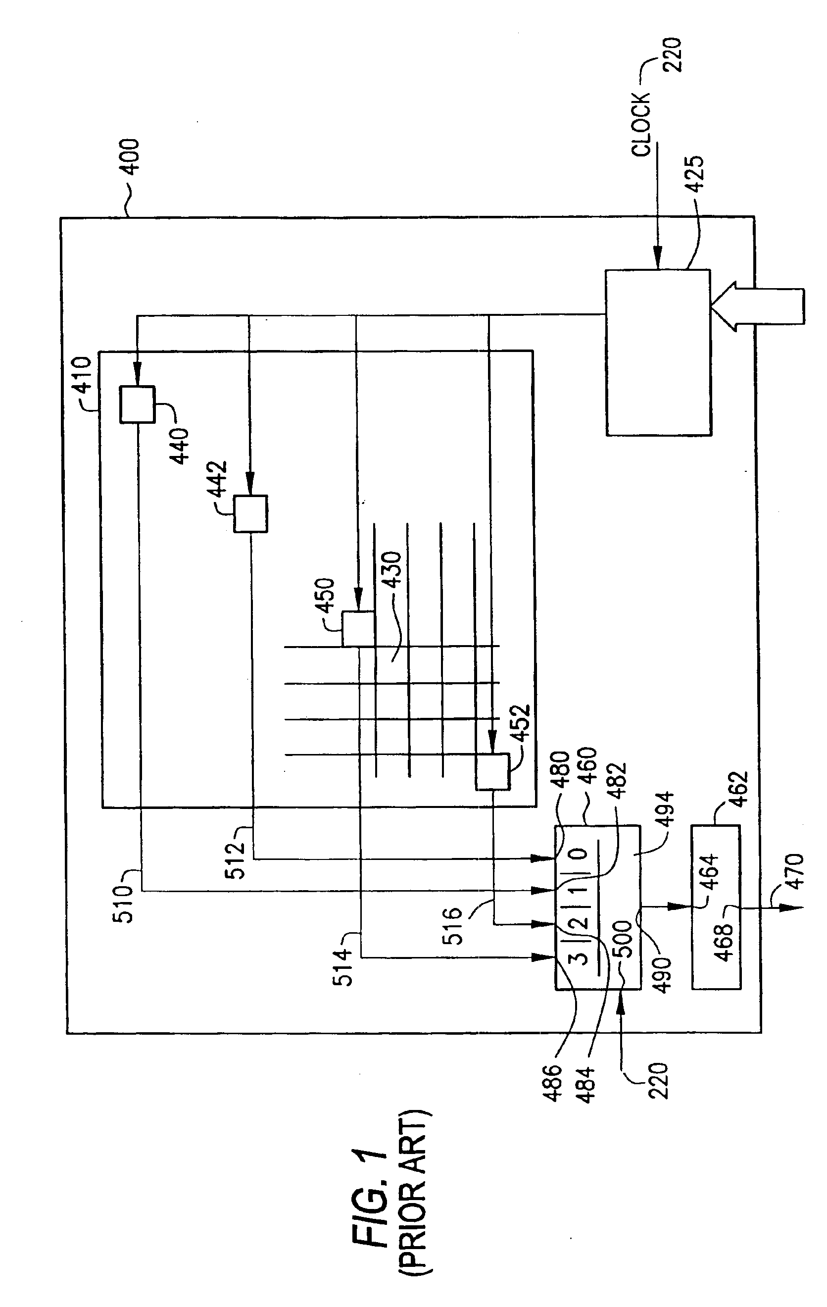
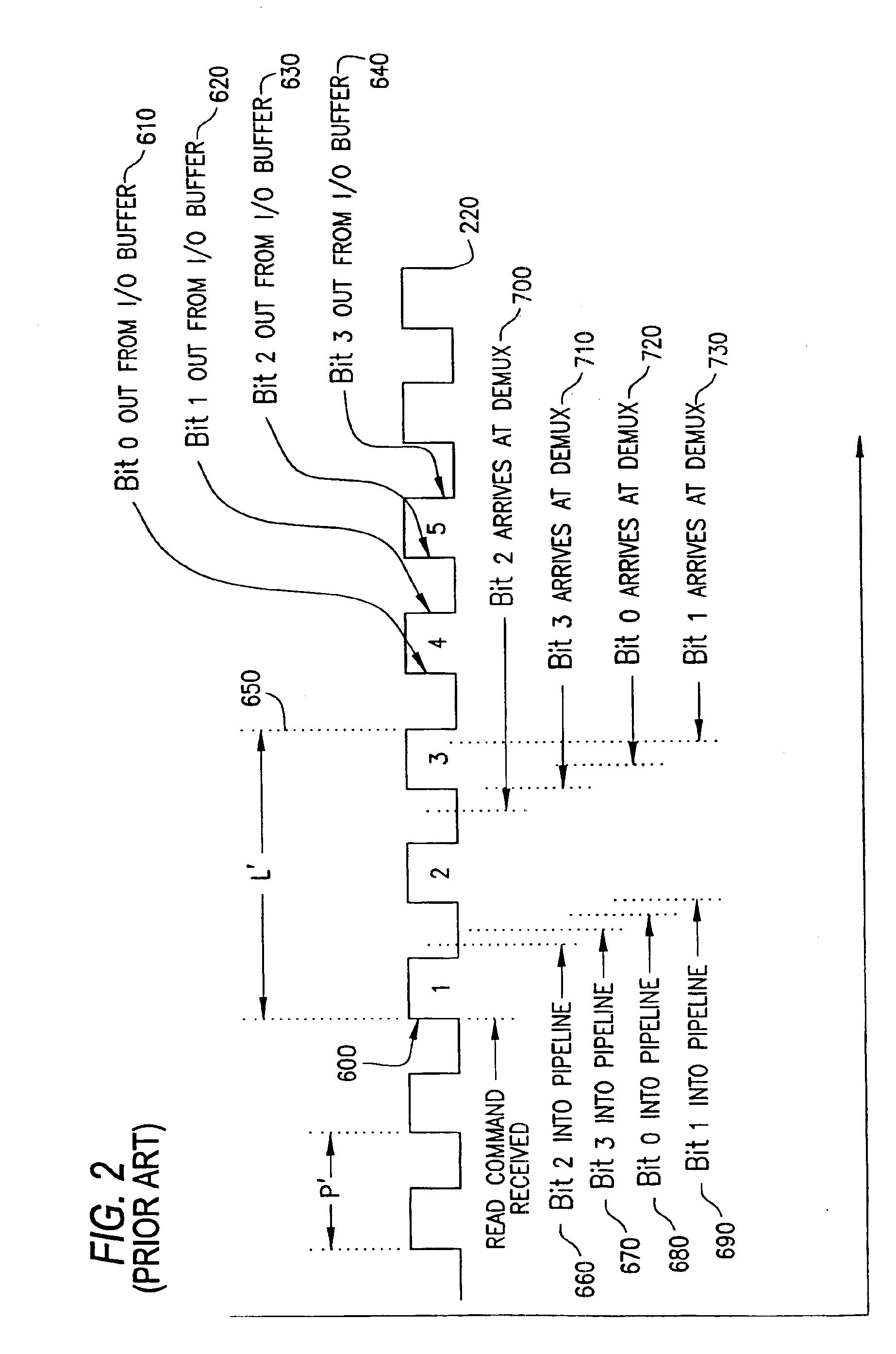
FIG. 1 illustrates, in simplified form, a conventional fourth order memory system. In the fourth-order memory architecture, four bits are selected from a single data quadrant (DQ) and routed to an output buffer in response to every read request. After arriving at the output buffer, these bits are output at subsequent rising and falling edges of a clock signal. Accordingly, FIG. 1 shows a memory integrated circuit 400 including a memory array DQ 410 made up of a large number of substantially identical cells 430. Four particular cells are identified as 440 and 442, 450 and 452, respectively.

An address decoder 425 is operatively connected to the array DQ 410 for selecting cells. As noted above, one of skill in the ar...


PUM


Abstract

A method and apparatus for storing and retrieving data in a second, or higher, order prefetch architecture memory integrated circuit. The method includes storing multiple bits of data in memory cells at various electrical distances from an output buffer and retrieving those memory bits concurrently for output. By outputting the bits in a fixed burst order, according to which a bit from a memory cell closer to the output buffer is output before a bit from a memory cell farther from the output buffer, the output time of the data bit from the closer memory cell can be used to mask a portion of the transit time of the bit from the farther memory cell. The apparatus includes memory cells at various locations for storing data bits, an address decoder adapted to store and retrieve multiple bits in a fixed burst order, and a multiplexer.

Description

BACKGROUND OF THE INVENTION1. Field of the InventionThe present invention relates generally to digital memory devices and, more particularly, to semiconductor memory devices that store and retrieve data from memory cells according to a fixed data burst order.2. Description of the Related ArtA digital memory, such as a dynamic random access memory (DRAM) has a memory array consisting of a number of individual m-bits or memory cells. Each working cell is adapted to store one binary digit (bit) of data. In a conventional DRAM device each memory cell consists of one transistor and one capacitor. A terminal of the transistor is connected to a column line (or digit line) of the memory device. Another terminal of the transistor is connected to a terminal of the capacitor and the gate terminal of the transistor is connected to a row line of the memory device. The transistor acts as a gate between the column line and the capacitor. When data is read from the cell, the terminal of the capacit...

Claims


Application Information

Patent Timeline
IPC IPC(8): G11C7/10
CPCG11C7/1039G11C7/106G11C7/1051G11C2207/107
Inventor STUBBS, ERIC T.
Owner MICRON TECH INC
Why Eureka
Try Eureka