Organic light-emitting display device

a display device and organic technology, applied in the direction of luminescnet screens, discharge tubes, identification means, etc., can solve the problems of low-speed response characteristics, narrow visibility angle, shortening the life of organic light-emitting devices, and generating variations in brightness in display devices, etc., to achieve the effect of reducing the resistance of wiring connected to an electrod

Inactive Publication Date: 2005-03-08
SAMSUNG DISPLAY CO LTD +1
View PDF4 Cites 60 Cited by
  • Summary
  • Abstract
  • Description
  • Claims
  • Application Information

AI Technical Summary

Benefits of technology

Accordingly, it is an object of the present invention to provide an organic light-emitting display device in which variations in brightness due to the resistance of wiring connected to an electrode of an organic light-emitting device can be reduced, as well as a method of manufacturing the organic light-emitting display device.
It is another object of the present invention to provide an organic light-emitting display device in which the deterioration of image quality due to the resistance of the wiring can be reduced, as well as a method of manufacturing the organic light-emitting display device.
According to the above-mentioned means, at least the electrode on one side of one organic light-emitting device belonging to each pixel is connected to the current supply line in a display region of each pixel, so that the wiring resistance of the current supply lines for connecting the electrodes on one side of the organic light-emitting devices and a power source is uniform for each pixel, and the wiring resistance in each pixel is negligibly small; therefore, variations in brightness due to the resistance of the wiring for connecting the electrodes of the organic light-emitting devices and the power source can be reduced, and variations in the brightness in the display region can be suppressed.
The electron injection layer herein is used for enhancing the efficiency of electron injection from the cathode into the electron transport layer. Desirable specific examples of the material of the electron injection layer include lithium fluoride, magnesium fluoride, calcium fluoride, strontium fluoride, barium fluoride, magnesium oxide, and aluminum oxide. Naturally, these materials are not limitative, and these materials may be used in a combination of two or more thereof.
The protective layer herein is formed on the second electrode, for the purpose of preventing H2O and O2 in the atmosphere from penetrating into the second electrode or into the organic layer provided under the second electrode.

Problems solved by technology

Such planar type display devices have used liquid crystal displays; however, liquid crystal display devices have problems in that they have a narrow angle of visibility and low-speed response characteristics.
Thus, there is the problem that the life of the organic light-emitting devices is shortened.
In addition, since the organic light-emitting devices are driven by an electric current, the voltage drop due to the wiring resistance is generated, and the voltage cannot be uniformly impressed on each of the pixels, particularly in the case of a large screen, with the result that variations in brightness are produced in the display device.
Thus, the simple matrix organic light-emitting display device has limitations as to enhancement of the definition and enlargement of the screen.
In the conventional organic light-emitting display devices, the light being emitted is taken out from the back side of the substrate, and therefore, an aperture ratio is limited in the active matrix organic light-emitting display device in which a driving portion is provided between the substrate and the organic light-emitting device.
Therefore, enlargement of the size of the panel poses a problem with the high resistance of the electrode.

Method used


Image

  • Organic light-emitting display device
  • Organic light-emitting display device
  • Organic light-emitting display device

Examples


embodiment 1

[Embodiment 1]

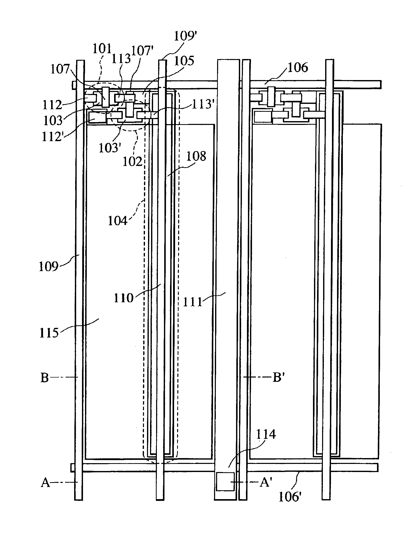
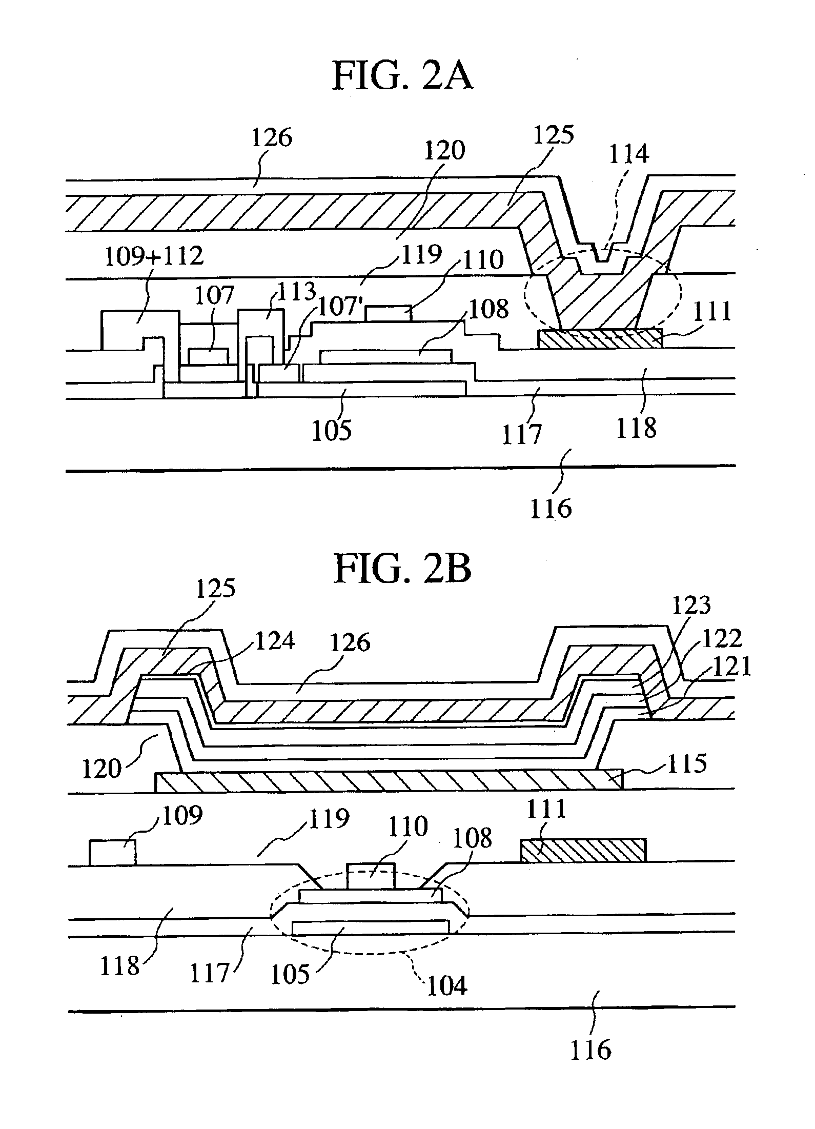
An organic light-emitting display system according to a first embodiment of the present invention will be described below with reference to the drawings. FIG. 1 is a plan view of a pixel in the organic light-emitting display device; FIG. 2A is a sectional view taken along line A-A′ of FIG. 1; and FIG. 2B is a sectional view taken along line B-B′ of FIG. 1. In FIGS. 1, 2A and 2B, a plurality of scanning lines 106, 106′ are disposed at a predetermined interval on a glass substrate 116, and signal lines 109, 109′, 109″ for transmitting picture data and the like are disposed at a predetermined interval in a direction orthogonal to each of the scanning lines. That is, the scanning lines and the signal lines are arranged in a grid form, and the region surrounded by a pair of the scanning lines and a pair of the signal lines constitutes a display region for one pixel. On the glass substrate 116, a plurality of first current supply lines 110 connected to a plus terminal of a p...

embodiment 2

[Embodiment 2]

A full color organic light-emitting display device according to a second embodiment of the present invention will be described with reference to FIGS. 4 and 5. This display device comprises a second current supply line and a feeding point at a lower portion of a green emission pixel region, and it has a high efficiency and a long life. FIG. 4 is a plan view of a pixel of an organic light-emitting display device according to this embodiment, and FIG. 5 is a sectional view taken along line A-A′ of the pixel region shown in FIG. 4.

The present embodiment has a structure in which, to display a color picture, a plurality of pixels serving as minimum units of the color picture are provided; green, red and blue organic light-emitting devices are provided as sub-pixels constituting each pixel; and a second electrode 125 of the organic light-emitting device of each pixel is connected to a second current supply line 111 in the display region of the green organic light-emitting de...

embodiment 3

[Embodiment 3]

A full-color organic light-emitting display device according to a third embodiment of the present invention will be described with reference to FIGS. 6 and 7. This display device, which comprises a second current supply line and a feeding point at a lower portion of a green light emission pixel region, is so constructed as to take out light from the back side of a substrate, and has a high efficiency and a long life. FIG. 6 is a plan view of a pixel of the organic light-emitting display device in this embodiment, and FIG. 7 is a sectional view taken along line A-A′ of FIG. 6.

In this embodiment, a sealing substrate 309 for the purpose of preventing water, oxygen and the like gases in the atmosphere from penetrating into a second electrode 125, an organic layer under the second electrode, or the interface between the second electrode and the organic layer is provided on the upper side of the second electrode 125, the other constitutions being substantially the same as in...


PUM


Abstract

A scanning line, signal line, first current supply line, and second current supply line are formed on a glass substrate. A first electrode is formed thereon; and, an organic layer, including a hole transport layer, light-emitting layer, electron transport layer, and electron injection layer is formed on the first electrode. A second electrode is formed as a cathode on the electron injection layer. The first electrode, serving as an anode, is connected to a plus terminal of a power source through driving devices and first current supply line, whereas the second electrode is connected to a minus terminal of the power source and is connected to the second current supply line in the display region of each pixel, with a contact hole serving as a feeding point, whereby the wiring resistance of the second electrode is reduced, and variations in the brightness of the panel is reduced.

Description

BACKGROUND OF THE INVENTIONThe present invention relates in general to an organic light-emitting display device; and, more particularly, the invention relates to a display device that is preferable for use in displaying pictures by means of organic light-emitting devices.Planar type display devices of the type used as man-machine interfaces have received increased attention with the advent of the real multi-media age. Such planar type display devices have used liquid crystal displays; however, liquid crystal display devices have problems in that they have a narrow angle of visibility and low-speed response characteristics.In recent years, organic light-emitting display devices have been proposed as the next-generation planar type display device. In this regard, organic light-emitting display devices have such characteristics as excellent auto-light-emission, a wide angle of visibility, and a high-speed response.In such organic light-emitting display devices, pixels are formed by org...

Claims


Application Information

Patent Timeline
Patent Type & Authority Patents(United States)
IPC IPC(8): H01L27/32H01L27/28H01L51/50G09F9/30H01L51/52H05B33/10H05B33/12H05B33/26
CPCH01L27/3276H01L27/3211H01L2251/5315H01L51/5237H01L51/5234H10K59/352H10K59/131H10K50/828H10K50/841H10K2102/3026H05B33/26
Inventor ISHIHARA, SHINGOOUCHI, TAKAYUKIMIKAMI, TOSHIROMASUDA, KAZUHITOARATANI, SUKEKAZU
Owner SAMSUNG DISPLAY CO LTD
Why Eureka
Try Eureka