
Optical modulator module

a technology of optical modulator and module, which is applied in the direction of optical elements, instruments, semiconductor lasers, etc., can solve the problems of large and complex device construction, inability to modulate light effectively and stably, and small tolerance of alignmen

Inactive Publication Date: 2005-03-08
SUMITOMO OSAKA CEMENT CO LTD
View PDF2 Cites 19 Cited by
  • Summary
  • Abstract
  • Description
  • Claims
  • Application Information

AI Technical Summary

Benefits of technology

In accordance with the invention related to claim 1, same polarization rotating element can achieve to bring the plane of polarization of light from semiconductor laser to optimum plane of polarization in waveguide of the optical modulation device, and block the returning light from optical modulation device to semiconductor laser as function named “isolator”. Therefore, it will prevent the increase of device size and moreover, even when the plane of polarization of light from semiconductor laser and expected optimum plane of polarization of the incident ray to the optical modulation device differs, it can prevent the loss caused by the optical joint between semiconductor laser and light modulation device, because it is possible to bring together by the said polarization rotating element.
In accordance with the invention related to claim 9, it will make possible not only to fulfill the stable laser emission with keeping the given temperature of semiconductor laser, but also incident the light with suitable plane of polarization or appropriate convergence condition at all times to optical modulation device, even if the temperature variation by temperature control means for semiconductor laser affects the supporting member for light source.

Problems solved by technology

However, according to the recently speed-up and high-capacity of data transmission for wavelength multiplex of optical networking and so on, the construction of device is becoming huge and complex and so it is increasingly needed to integrate and minimize the main components.
As a result, the increase of coupling loss, or the change of the coupling loss will occur, which disables to modulate light effectively and stably.
Therefore, tolerance of alignment is very small; particularly there is a problem that the tolerance of alignment, which is vertical to the surface of package and so supporting the LN optical modulation device, is much smaller.

Method used


Image

  • Optical modulator module
  • Optical modulator module
  • Optical modulator module

Examples


Embodiment Construction

Hereinafter is the detailed description, using the suitable examples of the invention.

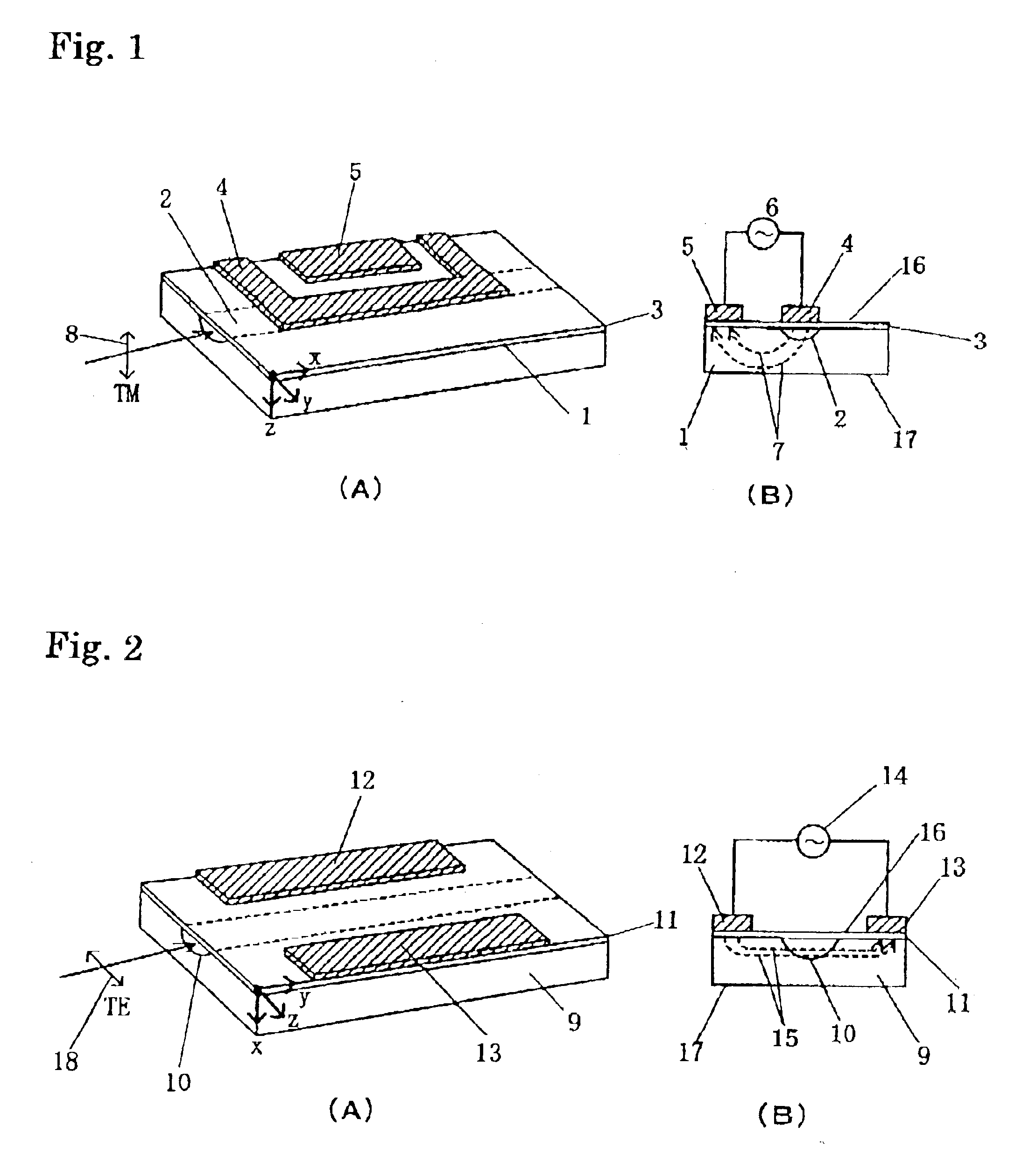
In order to comprise the optical modulator chip, the materials that contain electro-optical effect are preferable. For example, lithium niobate (LiNbO3: LN hereinafter), lithium tantaliate (LiTaO3), PLZT (lead lanthanum zirconate titanate), quartz system, and especially, LiNbO3 crystal, LiTaO3 crystal, or solid solution crystal structured by Lid and LiTaO3 are preferable, because they are easy to be made for light guide device and their anisotropy is bigger. In this practical example, the example mainly using lithium niobate (LN) is going to be explained.

In order to product optical modulator, Ti thermal diffusion above the LN chip constructs the light guide, and there are ways to construct electrode directly above the LN chip without placing the buffer layer on the whole chip or in some part, and another way to construct electrode for reducing the propagation loss of light inside the light wave gui...


PUM


Abstract

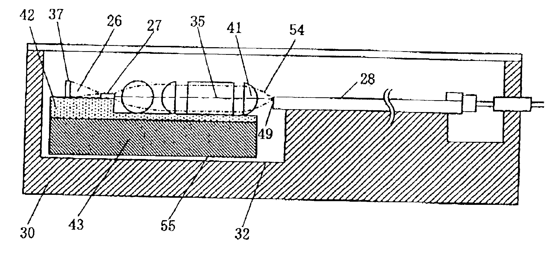
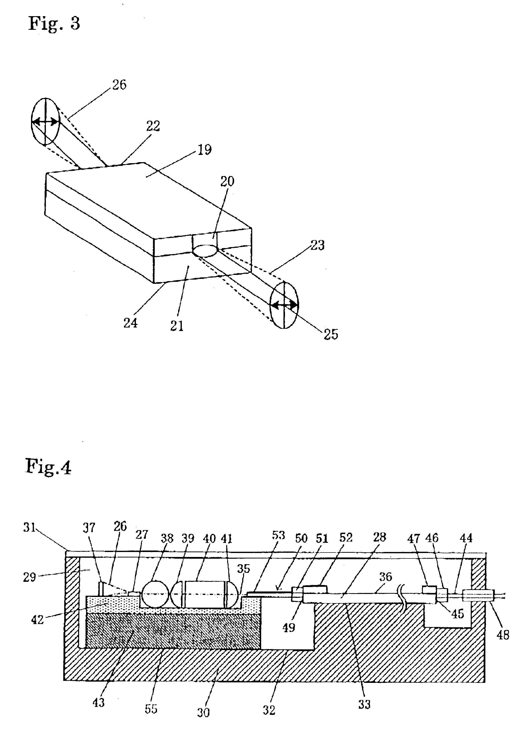
“This invention offer optical modulator module with fulfilling the effective and the stable optical modulation, which stabilizes the emission of semiconductor and control the shift of optic axis between the optical component by the temperature change and so on, when using the semiconductor laser. Peculiarly, the optical modulator module includes, in same package, the semiconductor laser (27) as light source, the optical modulation device (28) that has optical waveguide on the surface of the chip made by the element of the electro-optical effect, and the polarization rotating element (40) between said semiconductor laser and said optical modulation device, for bringing plane of polarization of light from said semiconductor laser (27) to optimum plane of polarization in waveguide of the said optical modulation device in line and blocking the returning light from said optical modulation device to said semiconductor laser.”

Description

BACKGROUND OF THE INVENTION(1) Field of the InventionThe present invention relates to an optical modulator module that includes light source and optical modulation device in the same package, and particularly to an optical modulator module that has the semiconductor laser as a light source.(2) Related Art StatementIn the field of advanced optical communication, the distributed feed back semiconductor laser (DFB laser) that have stable wavelength with narrow spectrum width are commonly used as light source and generates continuous wave (CW) and the laser beam is modulated responding transmission data by the optical modulator, which is placed in external side of the semiconductor laser and the modulated light is sent by the transmission line such as optical fiber.Moreover, the optical modulator, in most cases has the light guides on the surface of the chip made of the material of electro-optical effect, such as LiNbO3 (LN hereinafter), and electrodes near the light guides that high-sp...

Claims


Application Information

Patent Timeline
IPC IPC(8): H01S5/00H01S5/022G02B6/12G02B6/42G02F1/035
CPCG02B6/4208H01S5/02248H01S5/0085H01S5/02284H01S5/02208H01S5/02251H01S5/02325
Inventor SAKANE, TOSHIOSAITOU, TSUTOMUMURATA, SUSUMU
Owner SUMITOMO OSAKA CEMENT CO LTD
Learn More