
Bond pad structure comprising tungsten or tungsten compound layer on top of metallization level

a technology of bonding pad and compound layer, which is applied in the direction of natural mineral layered products, water-setting substance layered products, transportation and packaging, etc., can solve the problem that the bonding pad of the ic chip tends to deteriorate from damages

Inactive Publication Date: 2005-03-15
INFINEON TECH AG
View PDF21 Cites 9 Cited by
  • Summary
  • Abstract
  • Description
  • Claims
  • Application Information

AI Technical Summary

Benefits of technology

The present invention relates to a method for making an IC or DRAM cell device or chip with a fuse. The method involves using W or its compounds as a top or redundancy layer on top of Al or its alloy, which acts as the bond pad material. This results in a faster and more complete removal of the final passivation over the bond area during plasma etching, as compared to using titanium or its compounds. Additionally, W or its compounds can also function as an anti-reflective coating during lithography. The use of W or its compounds as a top metal or redundancy layer on Al or its alloy provides improved reliability and performance of the resulting device or chip.

Problems solved by technology

This is so because, when the bond pad is manufactured, the bond pad of the IC chip tends to deteriorate from damages during later probe test procedures and wire bonding processing.

Method used


Image

  • Bond pad structure comprising tungsten or tungsten compound layer on top of metallization level
  • Bond pad structure comprising tungsten or tungsten compound layer on top of metallization level
  • Bond pad structure comprising tungsten or tungsten compound layer on top of metallization level

Examples


Embodiment Construction

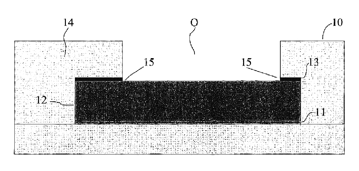
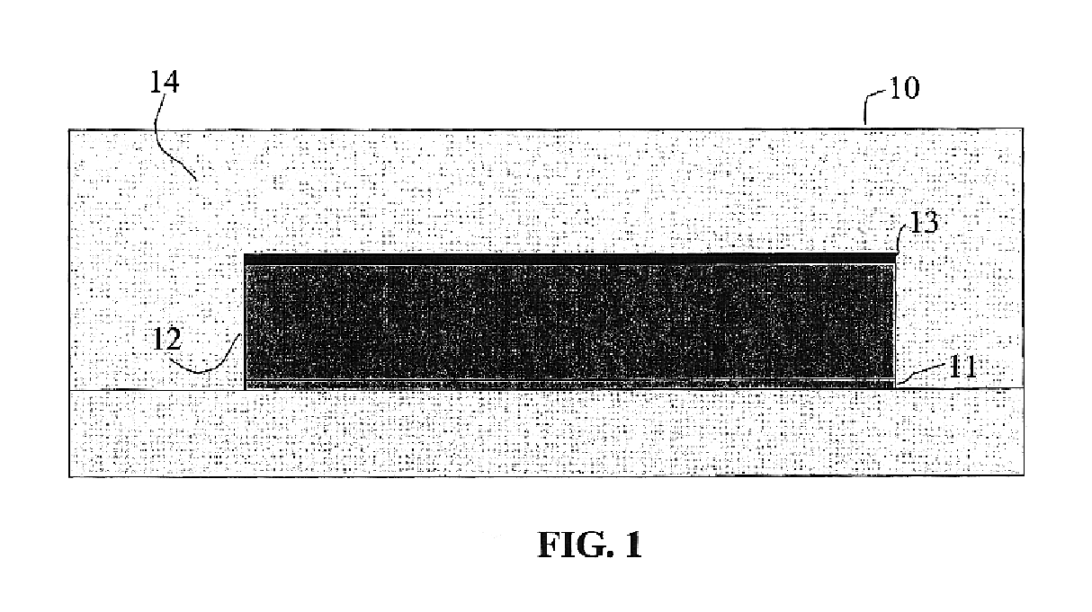
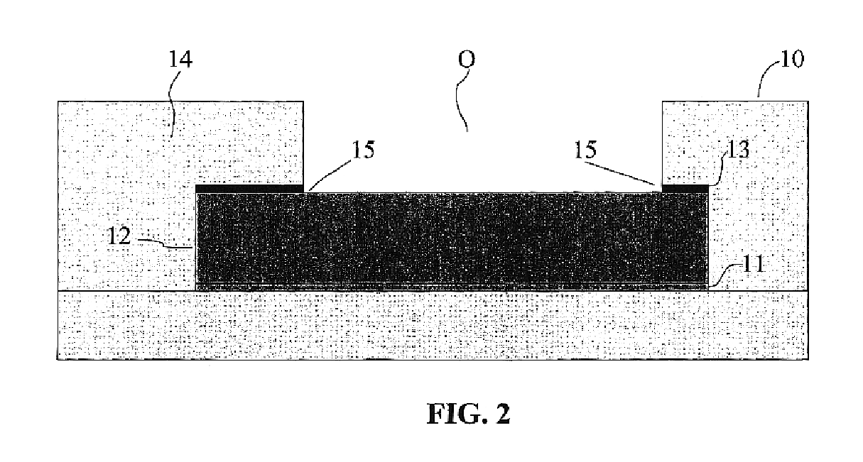
Reference is now-made to FIG. 1, which is a simplified cross sectional view of an integrated circuit (IC), DRAM cell device or chip 10, that may be formed in a polysilicon layer. In manufacturing this memory chip certain steps are taken to circumvent defective components and these steps may include additional segments of memory circuits provided on the IC chip as replacements for defective segments, and the way in which redundant segments are used and defective segments deleted is by use of laser trimming.

The IC chip structure of FIG. 1 comprises a conventional Ti based liner 11 and a metal layer 12 of Al or an Al compound, such as AlCu deposited thereon for purposes of forming a bond. Suitable Ti based liner material include, as examples only, Ti, TiN and TiW. Another suitable aluminum-based metal layer 12 is AlCuSi. A redundancy layer 13 (present on top of interconnecting line) which may be deposited by sputtering, is deposited on layer 12; however, in the context of the invention...


PUM

PropertyMeasurementUnit
areaaaaaaaaaaa
bond pad structureaaaaaaaaaa
thickaaaaaaaaaa

Abstract

A bond pad structure formed over a predetermined area of an IC substrate comprising quickly and easily removable redundancy and passivation layers upon lithography and plasma etching in a plasma containing Cl2, the bond structure comprises: a liner or lower metal layer formed on a predetermined area of the IC substrate; an aluminum-based metal layer formed on the liner layer as the last metal layer for bond purposes; a tungsten based redundancy layer formed on top of the aluminum-based last metal layer; and a passivation layer formed over the IC substrate and on the tungsten based redundancy layer.

Description

BACKGROUND OF THE INVENTION1. Field of InventionThe invention relates to bond pad structures for integrated circuits (IC) or semiconductor devices that use Al as the last metal for bond purposes, and employs tungsten or a tungsten compound layer as the top layer of the last metal stack, and wherein the tungsten or tungsten compound layer may function as a redundancy or anti-reflecting coat on top of the top metallization layer in the bond pad structure.2. Description of the Prior ArtA passivation layer etching process for memory arrays with fusable links is disclosed in U.S. Pat. No. 6,180,503 B1. The memory arrays with fusable links are obtained by etching the laser access opening in two steps using a transient etch stop layer between the first and second step. After a fuse is formed in a polysilicon level, an etch stop pad is patterned in a higher level metal or polysilicon level over the rupture zone of the fuse. The fuse access opening is then partially formed concurrent with a ...

Claims


Application Information

Patent Timeline
Patent Type & Authority Patents(United States)
IPC IPC(8): H01L23/485H01L23/48
CPCH01L24/02Y10T428/12535H01L2924/01006H01L2924/01013H01L2924/01014H01L2924/01022H01L2924/01029H01L2924/01047H01L2924/0105H01L2924/01056H01L2924/01074H01L2924/04941H01L2924/05042H01L2924/14H01L2924/01043Y10T428/12743Y10T428/12826Y10T428/12674Y10T428/1284H01L2924/01005H01L2924/12042H01L24/05H01L2224/04042H01L2924/00
Inventor FRIESE, GERALDROBL, WERNER K.BARTH, HANS-JOACHIMBRINTZINGER, AXEL
Owner INFINEON TECH AG
Learn More