Methods for fabricating final substrates

a technology of final substrates and substrates, applied in the direction of thin material processing, electrical equipment, semiconductor devices, etc., can solve the problems of relative longness and complexity

Inactive Publication Date: 2005-03-15
S O I TEC SILICON ON INSULATOR THECHNOLOGIES
View PDF13 Cites 171 Cited by
  • Summary
  • Abstract
  • Description
  • Claims
  • Application Information

AI Technical Summary

Benefits of technology

New and useful methods for fabricating final substrates for use in optics, electronics, or optoelectronics are described. In an embodiment, the method includes forming a zone of weakness beneath a surface of a source substrate to define a transfer layer, and preferably forming a first bonding layer on the source substrate surface. A second bonding layer may be advantageously formed on a surface of an intermediate support, and the exposed surfaces of the first and second bonding layers joined to form a composite substrate. Next, the source substrate is preferably detached from the composite substrate along the zone of weakness to expose a surface of the transfer layer, and a support material is deposited onto the exposed surface of the transfer layer. The transfer layer and support material are then advantageously separated from the composite substrate by elimination of at least the first bonding layer to form the final substrate.

Problems solved by technology

Such preparation generally includes polishing, planarizing, physical-chemical treatment, fabrication of intermediate layers, and the like, which can be relatively lengthy and complex.

Method used


Image

  • Methods for fabricating final substrates
  • Methods for fabricating final substrates
  • Methods for fabricating final substrates

Examples


first embodiment

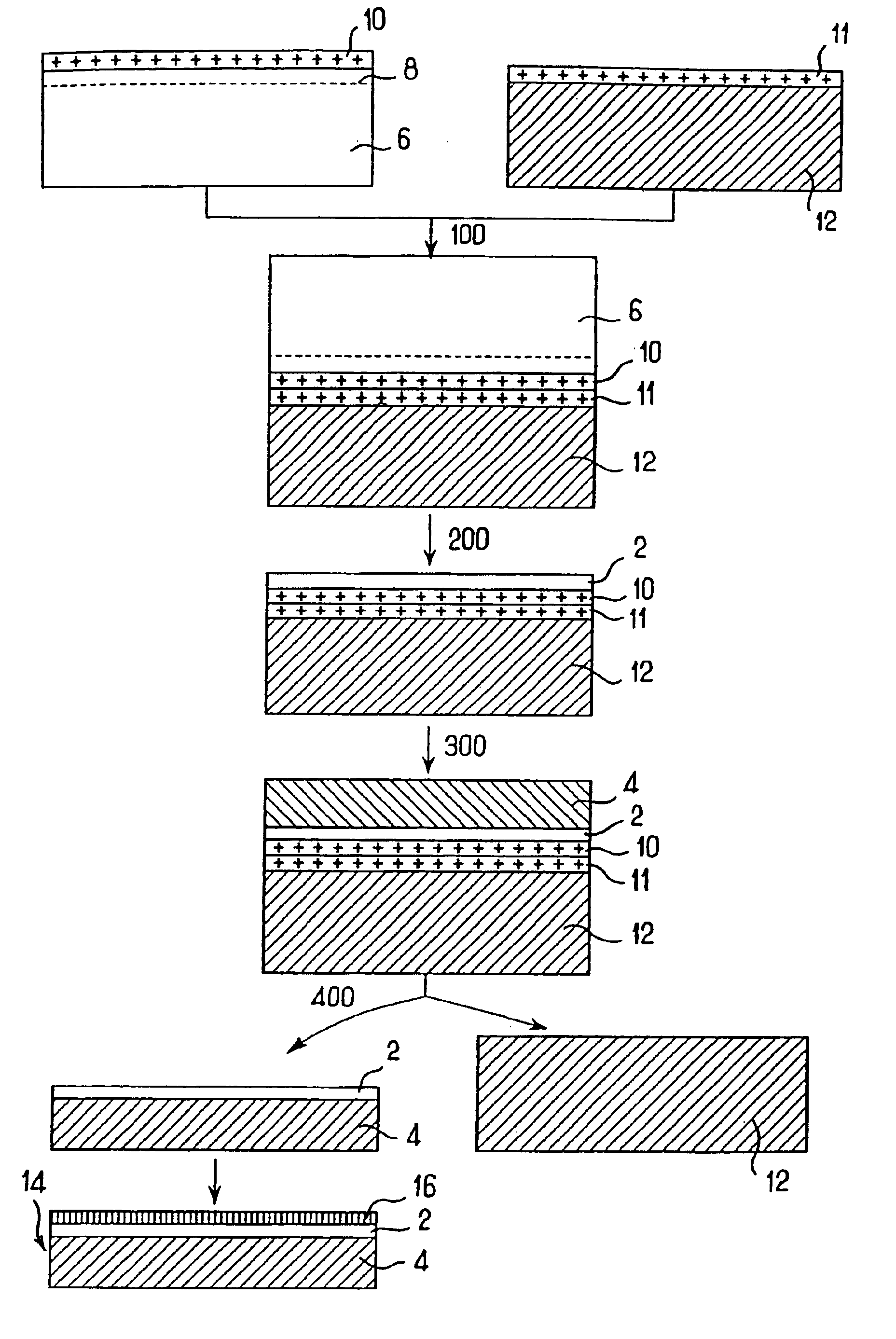
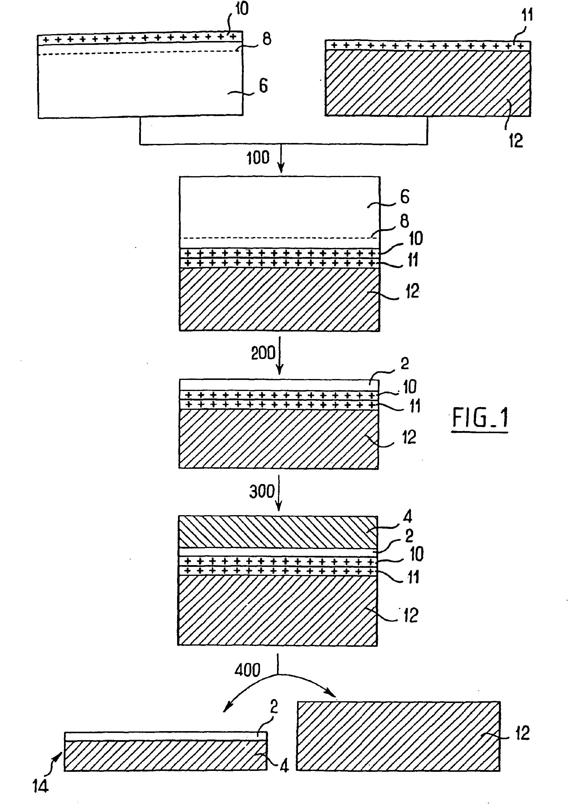
A number of non-limiting examples are now presented. The following table summarizes examples of materials that can be used for implementing the first embodiment described above.

TABLE 1IntermediateSupporting thickBonding layersThin layer 2support 12layer 410, 11Mono SiCPoly SiC orPoly SiC or polySiO2 or Si3N4mono SiCAlN or diamondor mono SiC ofquality inferior tothat of the thinlayerMono GaNPoly SiC or monoPoly SiC or polySiO2or Si3N4SiC or sapphireAlN or poly GaNor diamond ormono SiC ofquality inferior tothat of the thinlayer{111}, {1000}Poly Si or monoPoly Si or monoSiO2 or Si3N4etc. mono SiSi or poly SiC orSi of qualitymono SiCinferior to that ofthe thin layer

In the above table, as in the following tables, the term “mono” means “monocrystalline” and the term “poly” means “polycrystalline”.

example 1

The first example corresponds to the first row of Table 1.

The first implementation is particularly advantageous for forming a substrate comprising a thin transfer layer 2 of monocrystalline silicon carbide on a thick support material layer 4 of polycrystalline silicon carbide. Silicon carbide is difficult to obtain in single crystal form, even with diameters that are much smaller than those which are commonly obtained for single silicon crystals. This is due in particular to the fact that crystal-drawing techniques are more complex and expensive for monocrystalline silicon carbide than for monocrystalline silicon. In addition, the substrate forming steps are more difficult, more time consuming, and more expensive, for monocrystalline silicon carbide because of the unfavorable ratio between the hardness and the brittleness of silicon carbide. The present method is thus particularly advantageous for fabricating substrates with thin transfer layers 2 of silicon carbide since it enables...
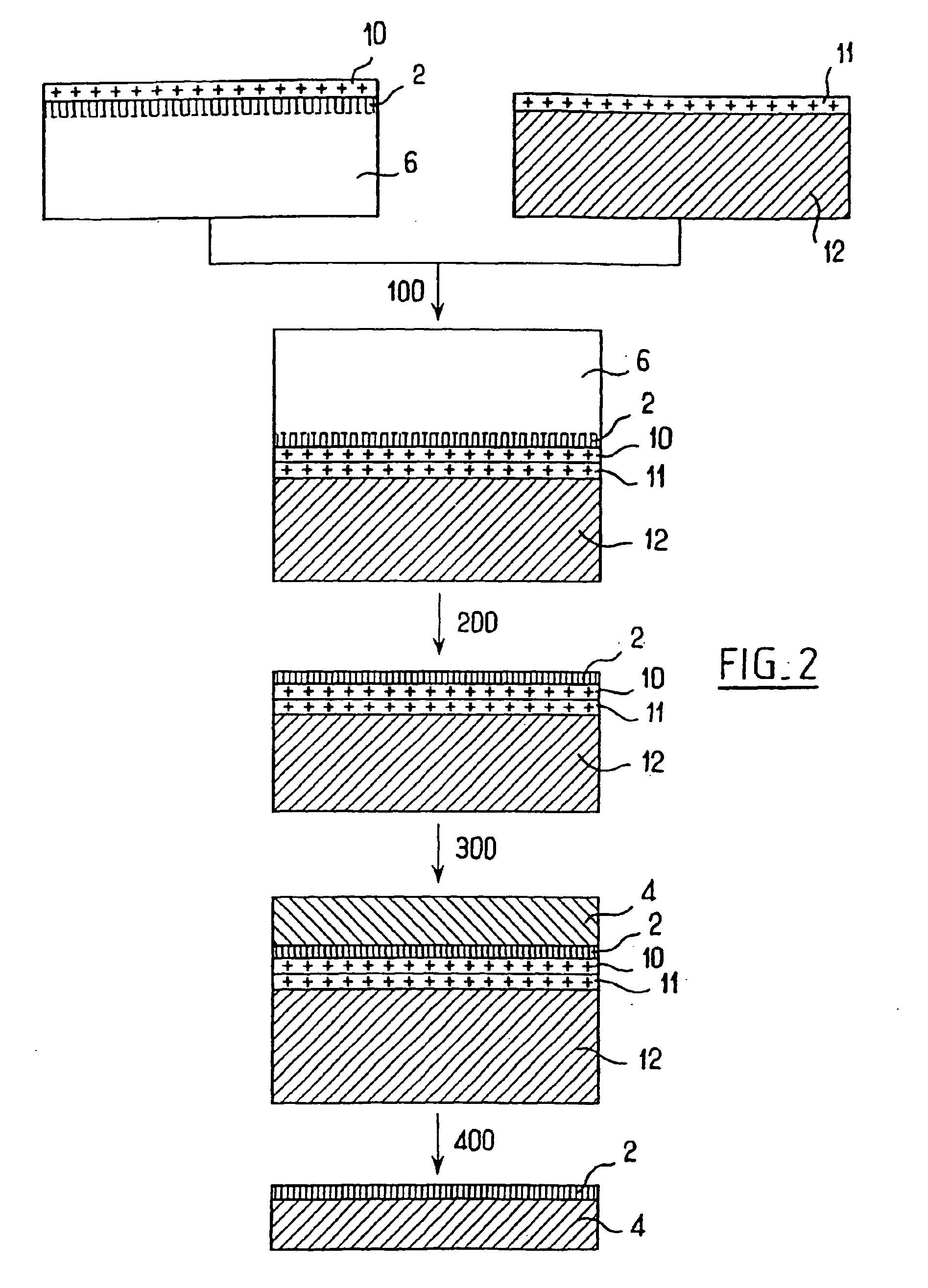
example 2

This second example corresponds to the second line of Table 1, and comprises the steps shown in FIG. 2. The operation includes depositing a thin layer 2 of monocrystalline gallium nitride on a source substrate 6 of monocrystalline silicon carbide by metal organic chemical vapor deposition (MOCVD) or by molecular beam epitaxy (MBE). A bonding layer 10 of silicon oxide is deposited on the thin layer 2, and a bonding layer 11 of silicon oxide is is deposited on an intermediate support 12 of polycrystalline silicon carbide. Next, in step 100, the two bonding layers 10 and 11 are placed in contact with each other, and bonded together. The method includes, in step 200, detaching the thin layer 2 of gallium nitride from the source substrate 6 via the interface between the thin transfer layer 2 and the source substrate 6 (e.g. by applying mechanical stresses) or via a zone of weakness made, for example, by implanting atomic species in the monocrystalline silicon carbide of the source substr...


PUM

PropertyMeasurementUnit
temperaturesaaaaaaaaaa
diameteraaaaaaaaaa

Abstract

Methods for fabricating final substrates for use in optics, electronics, or optoelectronics are described. In an embodiment, the method includes forming a zone of weakness beneath a surface of a source substrate to define a transfer layer, and forming a first bonding layer on the source substrate surface. A second bonding layer may be formed on a surface of an intermediate support, and the exposed surfaces of the first and second bonding layers joined to form a composite substrate. Next, the source substrate is detached from the composite substrate along the zone of weakness to expose a surface of the transfer layer, and a support material is deposited onto the exposed surface of the transfer layer. The transfer layer and support material are then separated from the composite substrate by elimination of at least the first bonding layer to form the final substrate. The zone of weakness may advantageously be formed by implanting atomic species into the source substrate.

Description

BACKGROUND ARTThe invention relates to methods of fabricating substrates, in particular for optics, electronics, or optoelectronics, and also to substrates obtained by such methods. More particularly, the substrates can be used to make microsystems, sensors, light-emitting or laser diodes, and the like.U.S. Pat. No. 5,374,564 discloses a method of fabricating substrates in which a thin layer of a material is transferred from a source substrate onto a support. The operation of bonding the thin layer to the support is often achieved by molecular adhesion, and in order to obtain a good adhesive interface the surfaces that are to be bonded together must be specially prepared prior to being brought into contact. Such preparation generally includes polishing, planarizing, physical-chemical treatment, fabrication of intermediate layers, and the like, which can be relatively lengthy and complex. This is particularly true when the supporting substrate is polycrystalline.Thus, improvements in...

Claims


Application Information

Patent Timeline
Patent Type & Authority Patents(United States)
IPC IPC(8): H01L21/762H01L21/70H01L29/267H01L29/02H01L29/165H01L29/24H01L29/20H01L27/12H01L21/02
CPCH01L21/3148H01L21/318H01L21/76254H01L29/165H01L29/267Y10T428/24479H01L29/2003H01L29/1608H01L21/02167H01L21/0217H01L21/34
Inventor GHYSELEN, BRUNOLETERTRE, FABRICE
Owner S O I TEC SILICON ON INSULATOR THECHNOLOGIES
Why Eureka
Try Eureka