

Stacked organic memory devices and methods of operating and fabricating
a memory device and organic technology, applied in thermoelectric devices, instruments, nanoinformatics, etc., can solve the problems of increasing the volume, use and complexity of computers and electronic devices, reducing the efficiency of data storage, so as to facilitate charge migration, reduce the cost and the effect of loss of data storage density
- Summary
- Abstract
- Description
- Claims
- Application Information
AI Technical Summary
Benefits of technology
Problems solved by technology
Method used
Image

Examples
Embodiment Construction
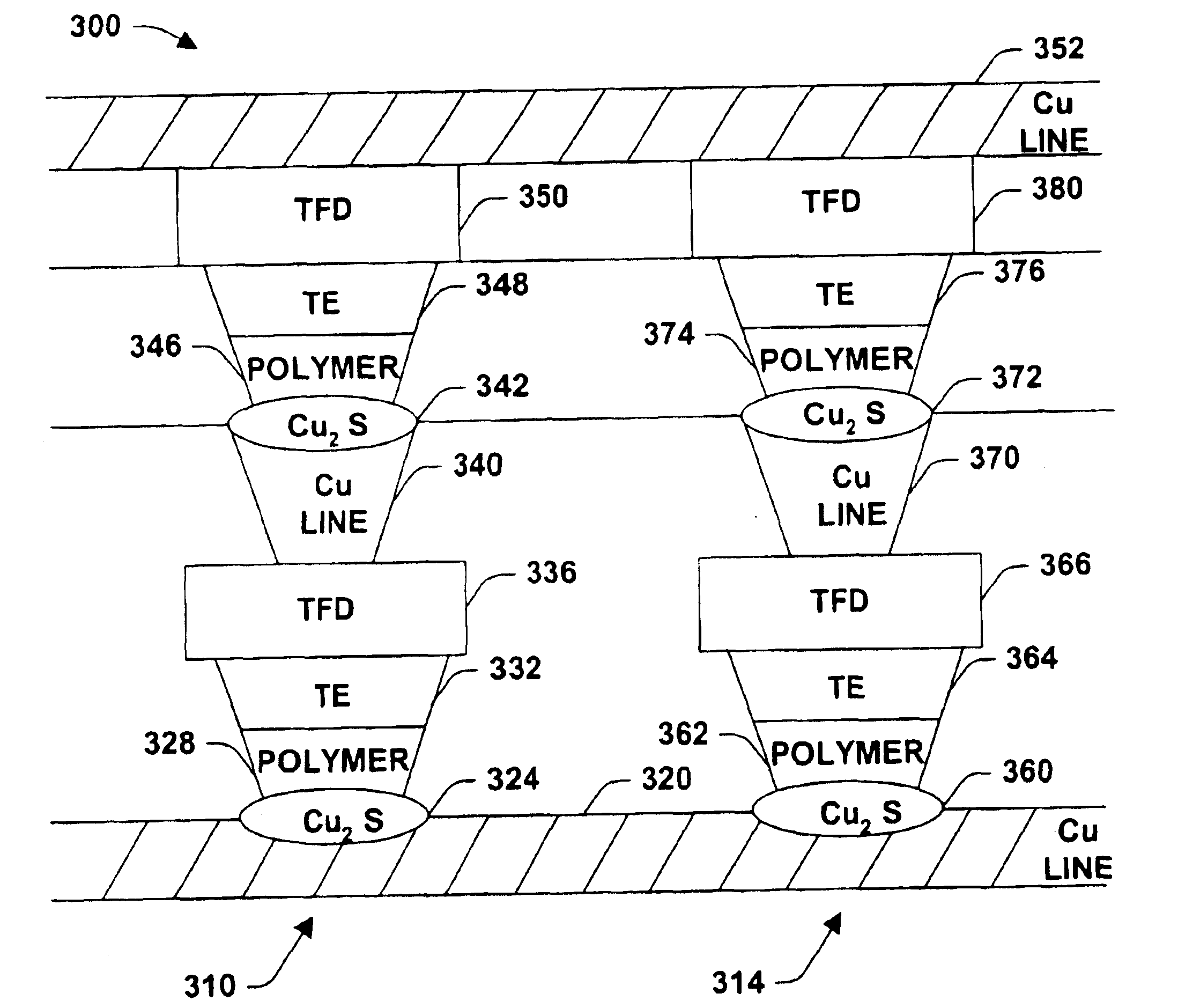
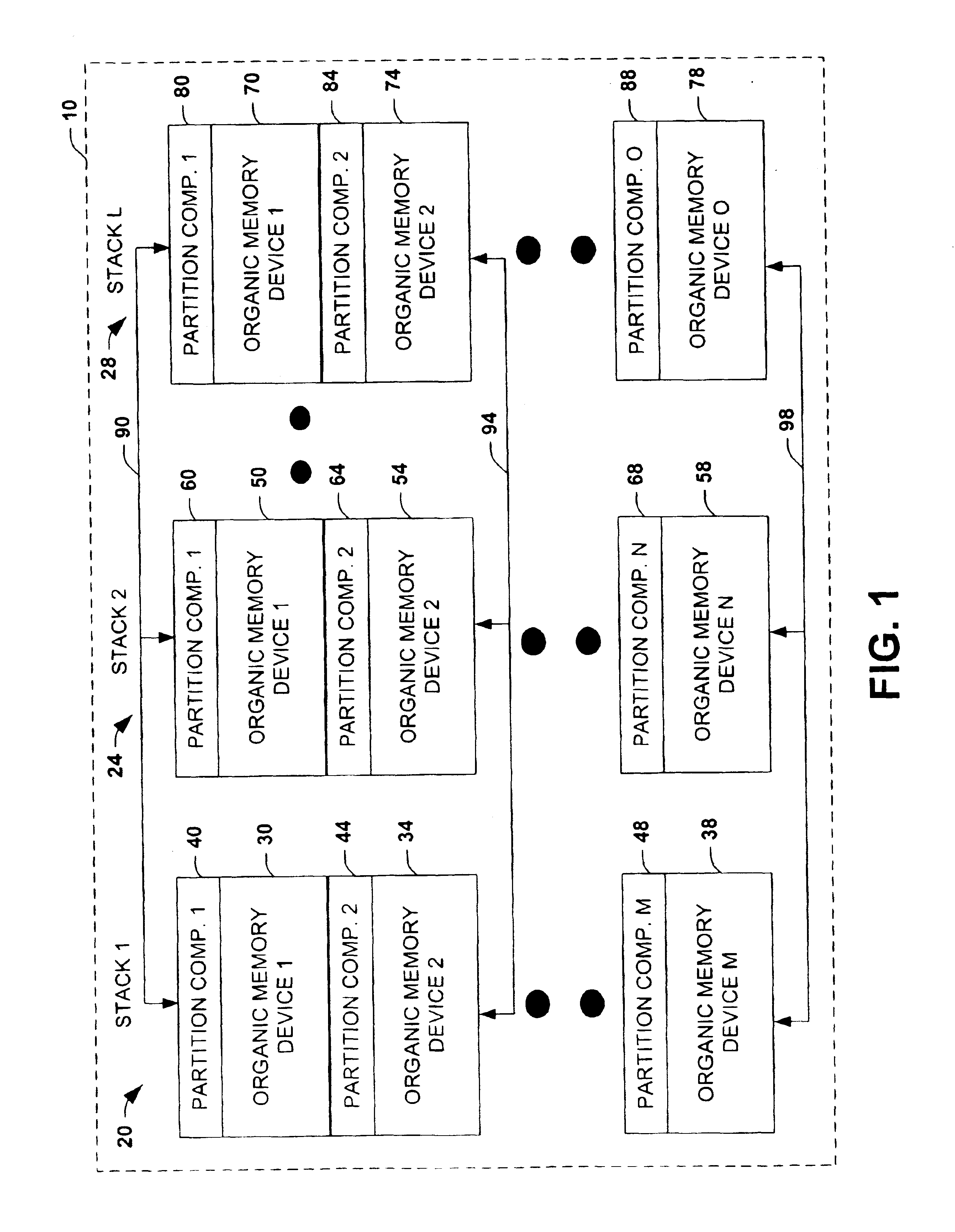
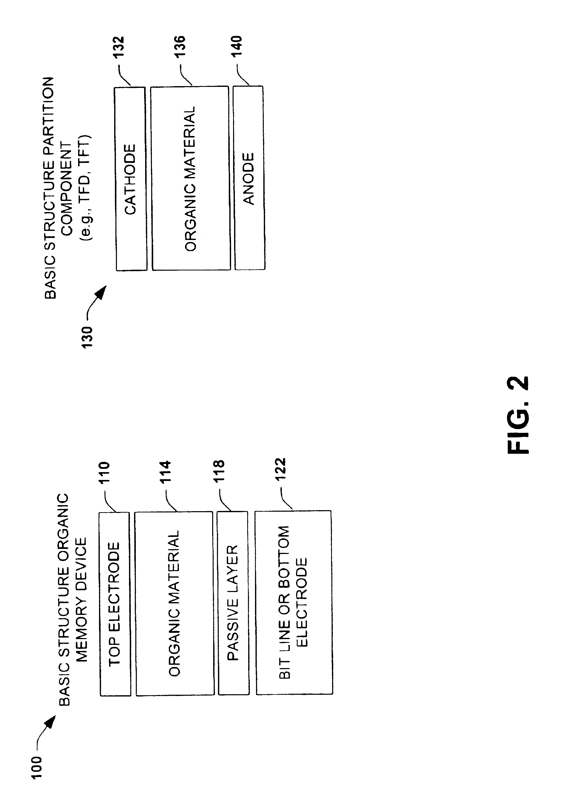
The present invention provides a multi-layer organic memory device that can operate as a non-volatile memory device having a plurality of stacked and / or parallel memory structures constructed therein. A multi-cell and multi-layer organic memory component can be formed with two or more electrodes having a selectively conductive media between the electrodes forming individual cells, while utilizing a partitioning component to enable stacking of additional memory cells on top of or in association with previously formed cells. Memory stacks can be formed by forming additional layers—respective layers separated by additional partitioning components, wherein multiple stacks can be formed in parallel to provide a high-density memory device. The selectively conductive media is formed in various portions of the memory structures which contains an organic conductor layer and one or more passive layers. The selectively conductive media is programmed (e.g., written) by applying bias voltages th...
PUM
| Property | Measurement | Unit |
|---|---|---|
| Digital information | aaaaa | aaaaa |
| Electrical conductor | aaaaa | aaaaa |
Abstract
Description
Claims
Application Information