Silicon-on-insulator biosensor device

a biosensor and silicon-on-insulator technology, applied in the direction of transistors, instruments, material analysis, etc., can solve the problems of lagging sensitivity and universality of general approaches, unable to meet the needs of sensitivity as well as hampered usability

Inactive Publication Date: 2005-03-22
FUJITSU LTD
View PDF9 Cites 112 Cited by
  • Summary
  • Abstract
  • Description
  • Claims
  • Application Information

AI Technical Summary

Problems solved by technology

Their usability is hampered by the need of highly insulating organic layers.
However, these approaches in general lack the sensitivity and universality.
Also, standard FET structures were proposed for the use of biosensors, but lacked the necessary sensitivity as well (e.g. Schöning and Lüth, 2001).
The techniques currently used mostly suffer from the need to use optical detection.
However, it introduces additional biochemical preparation steps, which results in the loss of significant parts of the material of interest.
This is a major drawback of these approaches, as especially for diagnostic purposes only very small quantities of the analyte are available.
All mentioned techniques based on silicon devices have resolution limits for very small protein concentrations.

Method used


Image

  • Silicon-on-insulator biosensor device
  • Silicon-on-insulator biosensor device
  • Silicon-on-insulator biosensor device

Examples


Embodiment Construction

Before beginning a detailed description of the subject invention, mention of the following is in order. When appropriate, like reference numerals and characters may be used to designate identical, corresponding or similar components in differing figure drawings. Further, in the detailed description to follow, exemplary sizes / models / values / ranges may be given, although the present invention is not limited to the same.

Although recent progress in Genomics and Proteomics enables the purification of a huge number of different biomolecules, very few techniques are available to detect, analyse and quantify these species and their mutual interactions. Progress in the current biomedical research is relying on new universal tools, which allow the identification of specific interactions between biomolecules in a highly parallel and highly sensitive way.

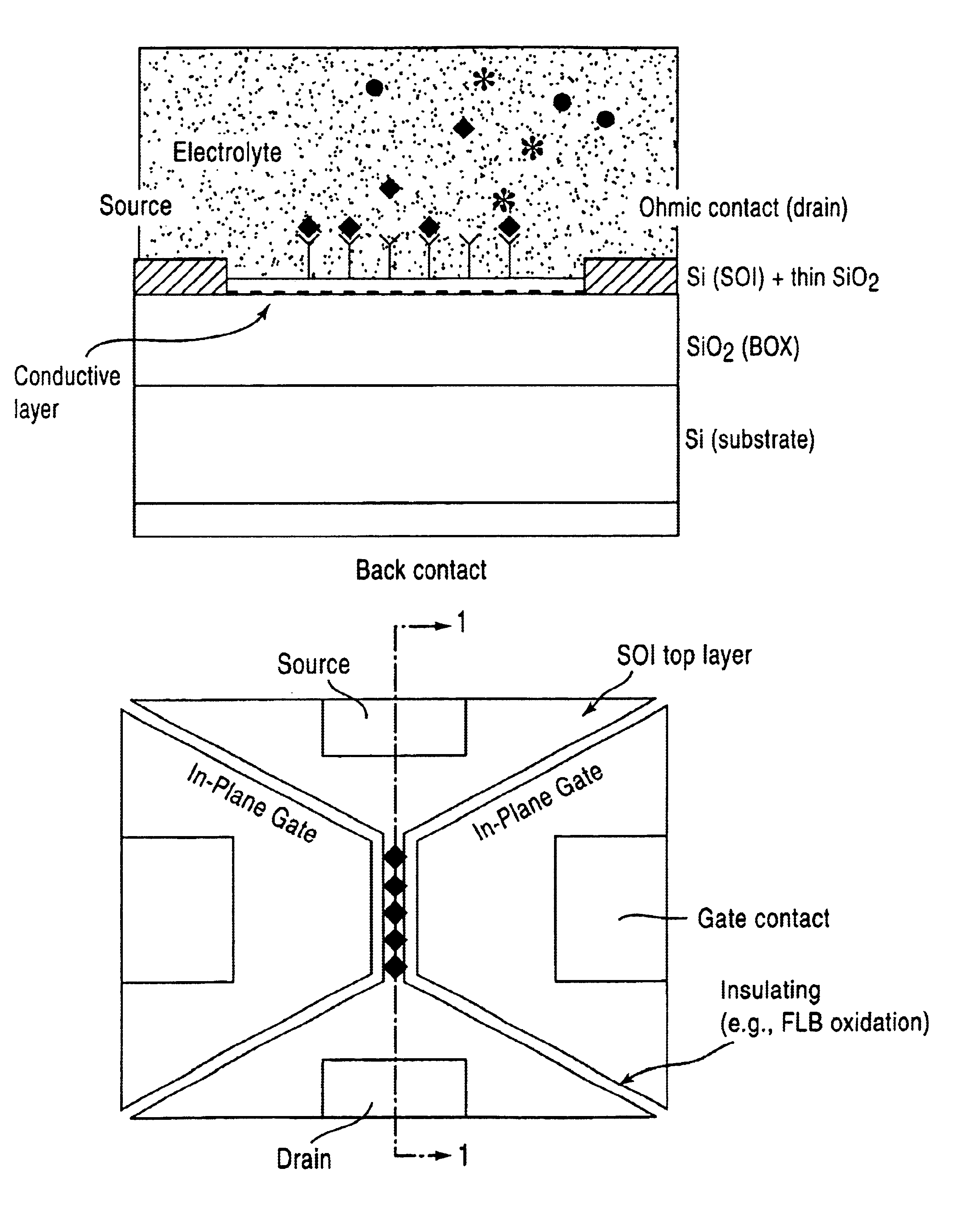
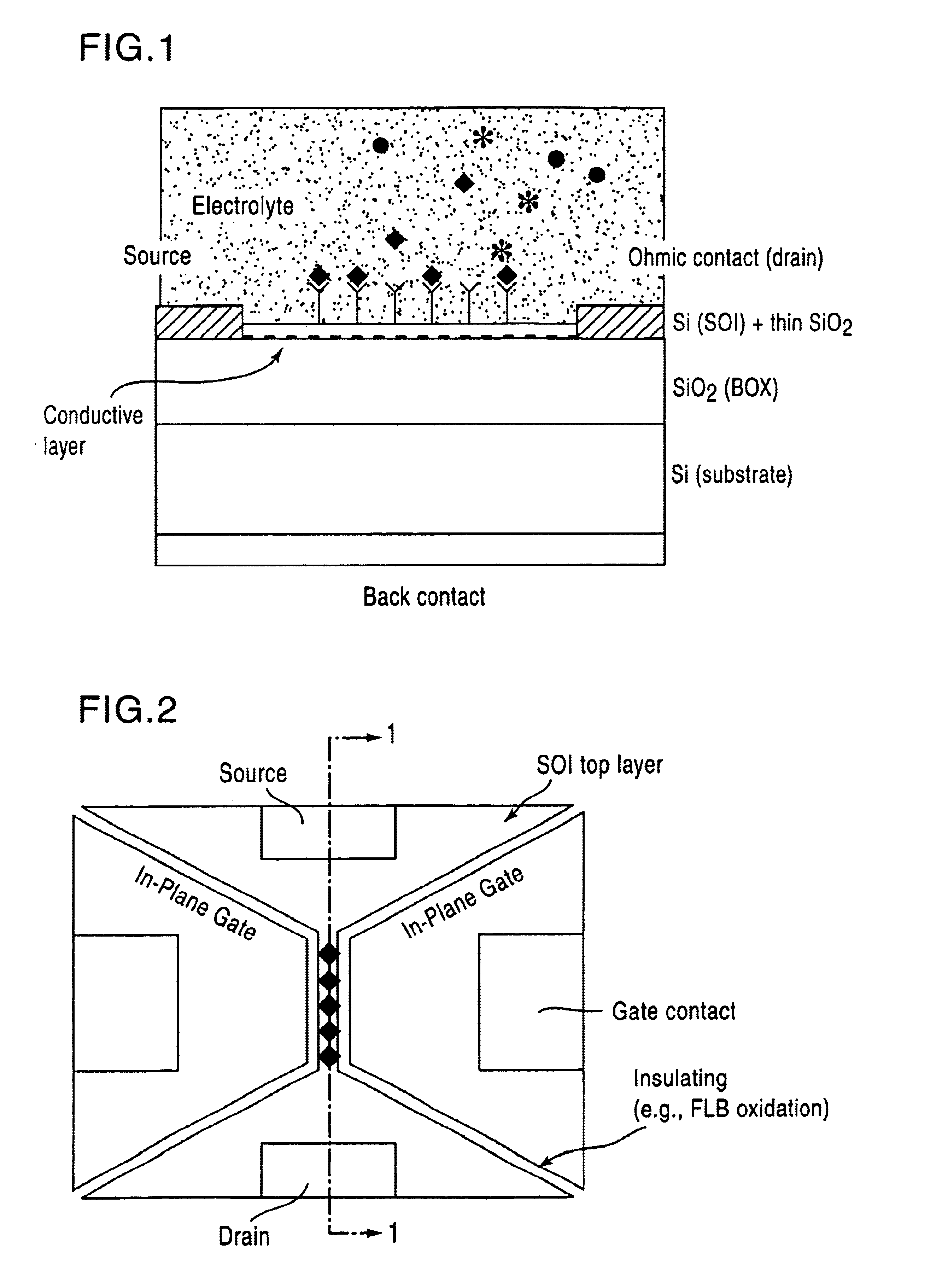
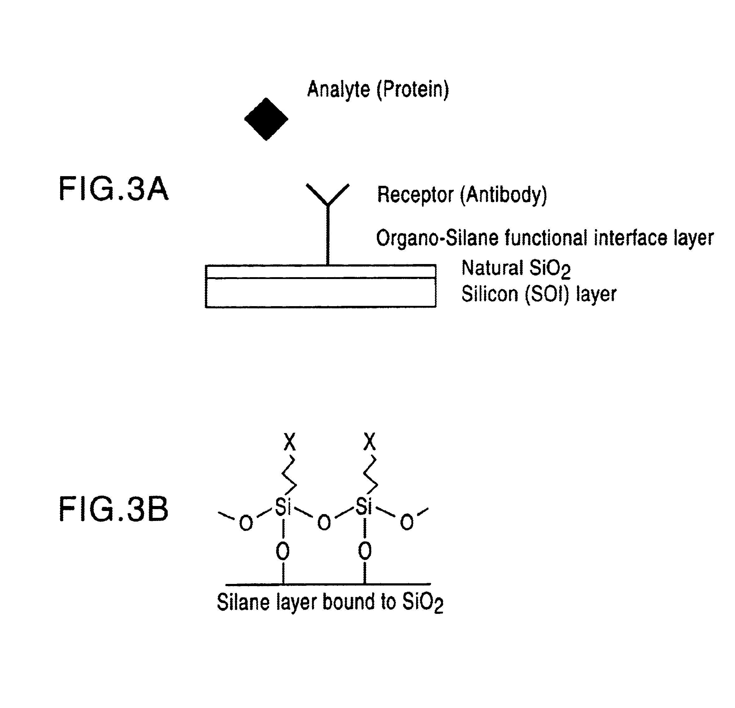
The invention covers a semiconductor device for the detection of specific biomolecular interactions based on Silicon-on-Insulator (SOI) technol...


PUM

PropertyMeasurementUnit
thicknessaaaaaaaaaa
thicknessaaaaaaaaaa
thicknessaaaaaaaaaa

Abstract

A Semiconductor sensor device for the detection of target molecules and molecular interactions, based on Silicon-on-Insulator (SOI) technology.

Description

FIELD OF THE INVENTIONThe present invention relates to a silicon-on-insulator biosensor device. Specifically, the present invention allows for the identification of specific interactions between biomolecules in a highly parallel and highly sensitive way.BACKGROUND OF THE INVENTIONCurrent techniques for protein detection, analysis and quantification include, e.g., two-dimensional gel electro-phoresis combined with mass spectroscopy, micro-capillary electrokinetic separation techniques with fluorescent read-out, micro-array analogs to DNA chip technology, and others like plasmon-resonance or quartz microbalance. In present micro-array approaches the underlying “chip” mostly consists of a surface functionalized plain glass substrate without any intrinsic function, detection hence relies solely on fluorescent labeling.A common approach using silicon structures for the detection of biomolecular interactions is the use of capacitive measurements (Berggren et al., Electroanalysis 2001). Th...

Claims


Application Information

Patent Timeline
Patent Type & Authority Patents(United States)
IPC IPC(8): G01N27/403G01N27/414
CPCG01N27/4145
Inventor ABSTREITER, GERHARDTORNOW, MARC UWEBUCHHOLZ, KARINLUBER, SEBASTIAN MARKUSSACKMANN, ERICHBAUSCH, ANDREAS RICHARDNIKOLAIDES, MICHAEL GEROLD HELLMUTRAUSCHENBACH, STEFAN
Owner FUJITSU LTD
Why Eureka
Try Eureka