Maskless lithography with multiplexed spatial light modulators

a spatial light modulator and maskless lithography technology, applied in the field of optical patterning system, can solve the problems of uneconomical changes by dmd manufacturers, significant area loss, and further damage to the above packing efficiency, and achieve the effect of improving throughpu

Inactive Publication Date: 2005-03-22
ANVIK CORP
View PDF2 Cites 56 Cited by
  • Summary
  • Abstract
  • Description
  • Claims
  • Application Information

AI Technical Summary

Benefits of technology

An advantage of the invention is that it is modular, and can be incorporated into a patterning system using a variety of configurations of DMDs or other SLMs.
Another advantage of the invention is that the focal length of the pixel-beams can vary by a large amount (as much as 5 mm) without adversely affecting the much more precise focus requirements at the image plane of the reducing projection lens and the surface of the substrate.
Still another advantage, a major enhanc

Problems solved by technology

While the active mirror portions of the DMD chips have very dense pixel packing, there are significant area losses due to kerf areas and fan-out boards.
The above packing efficiency is further

Method used


Image

  • Maskless lithography with multiplexed spatial light modulators
  • Maskless lithography with multiplexed spatial light modulators
  • Maskless lithography with multiplexed spatial light modulators

Examples


Embodiment Construction

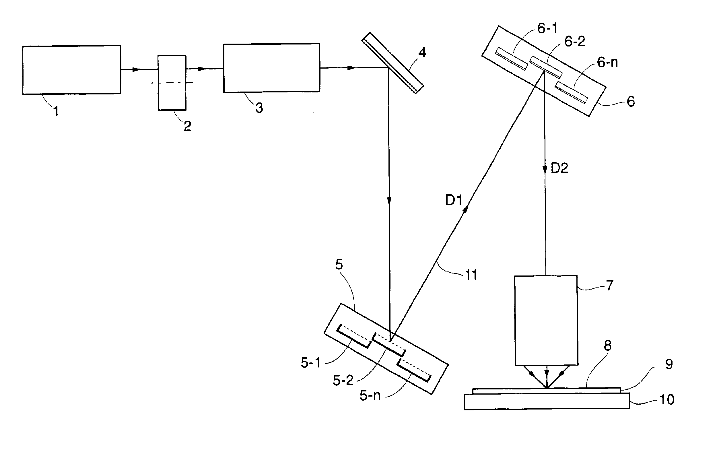
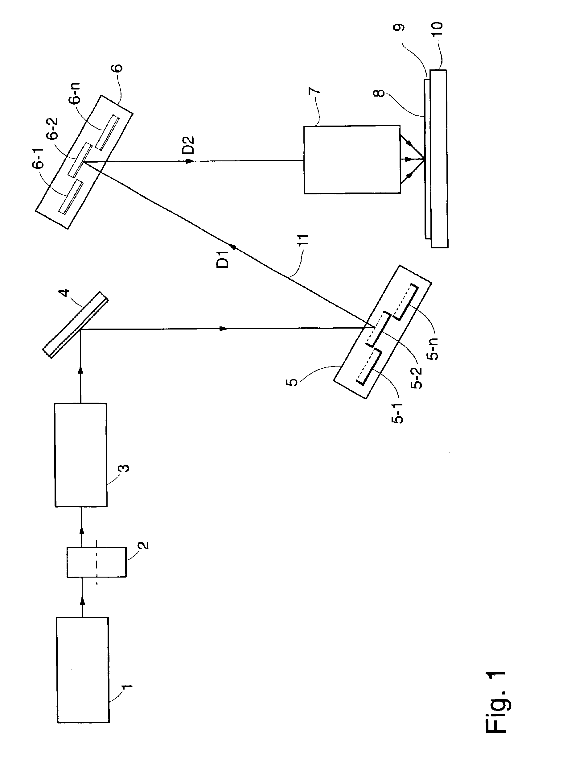
The multiplexed-SLM maskless lithography system is shown in FIG. 1. Light source 1, which may preferably be a pulsed excimer laser or a continuous-wave (CW) light source, such as a lamp or a gas laser, chopped by a pulser 2, provides illumination pulses. The pulser 2 may be a mechanical chopper or an optical shutter or an electro-optical modulator. The pulses are required in order to provide illumination synchronization with the pixel data. The pulses also provide blanking during the refresh portion of the cycle, during which various required scanning motions may be provided and during which the micromirror selection may be changed. The next system element is a beam conditioner 3, which preferably is a recycling homogenizer, to efficiently uniformize the full beam area. Steering mirror 4 redirects the full beam to the multiplexed SLM subsystem 5, which preferably is a twin-plane package of slightly-overlapped DMD arrays 5-1, 5-2 . . . 5-n. Each DMD array has some 800,000 micromirror...


PUM


Abstract

Imaging systems that use a spatial light modulator (SLM), such as maskless lithography systems using a digital micromirror device (DMD), suffer from low throughput at high resolution because of the increase in the number of pixels to be imaged. A possible solution to this problem is provided by using multiple SLMs. However, packaging multiple SLMs on a suitable base is inefficient because, in an SLM, surrounding the active region, a large inactive region is required for the chip kerf and the connector fan-in; these inactive regions thus prevent close packing of the SLMs. This invention enables close packing of a large number of SLMs by arranging them in twin planes, such that the kerf and fan-in regions overlap substantially. Variations in the optical conjugate distances of different SLMs caused by the twin planarity are eliminated by incorporation of a twin-pane compensating mirror array that corresponds to the SLM array, and introduces a pathlength difference between different mirrors that is complementary to the pathlength difference between corresponding SLM chips. Depth-of-focus problems are thus eliminated. The invention enables significant throughput enhancement, up to 82%, in maskless lithography systems.

Description

FIELD OF THE INVENTIONThe invention relates to an optical patterning system using multiple reflective spatial light modulator (RSLM) chips, and more particularly relates to a very high throughput, large-area maskless lithography system, using multiple RSLM chips mounted in plural planes with partial overlapping for closer RSLM chip packing and higher throughput, and using related auxiliary mirrors in complementary plural planes to compensate for pixel beamlet length variations from multi-planar RSLM chip placement.DESCRIPTION OF RELATED ARTA variety of spatial light modulator (SLM) types, some transmissive and some reflective, are currently available. Preferred is a reflective SLM (RSLM) of the digital micromirror device (DMD chip) in which an array of micromirrors mounted in an x-y array of rows and columns can serve as individually selectable multiple beam devices. Each micromirror element has an x-y address selected by electrical signals to remain flat when unselected, or tilt wh...

Claims


Application Information

Patent Timeline
IPC IPC(8): G03F7/20
CPCG03F7/70291G03F7/70283
Inventor JAIN, KANTI
Owner ANVIK CORP
Why Eureka
Try Eureka