Molecular memory cell

a memory cell and molecular technology, applied in the field of molecular memory cells, can solve the problems of complex silicon processing steps, still volatile, and loss of contents

Inactive Publication Date: 2005-03-29
ADVANCED MICRO DEVICES INC
View PDF112 Cites 14 Cited by
  • Summary
  • Abstract
  • Description
  • Claims
  • Application Information

AI Technical Summary

Benefits of technology

In accordance with another aspect of the present invention, a switching device comprises an active region having a high-impedance state and a low-impedance state and including a molecular matrix and ionic complexes distributed in the matrix, each of the ionic complexes being composed of at least a pair of ions having opposite charges. The active region is responsive to a switching signal for switching between the high-impedance state and the low-impedance state when the amplitude of the switching signal exceeds a threshold level determined based on the duration of the switching signal. In particular, the switching signal may cause displacement of the ions in the ionic complexes to switch the active region from the high-impedance state to the low-impedance state.
In accordance with a further aspect of the present invention, a method of switching a device of the present invention involves determining a threshold level for switching the device based on the duration of a switching signal for switching the device, and applying the switching signal having an amplitude exceeding the threshold level to switch the device between the high-impedance state and the low-impedance state.
In accordance with another aspect of the present invention, a memory cell comprises a pair of electrodes, and an active layer including a molecular system and ionic complexes distributed in the molecular system. The active layer is configured to enable writing information into the memory cell when the intensity of an electric field applied to the active layer exceeds a threshold value, and to enable reading information from the memory cell when the absolute value of the electric field intensity is no more than the threshold value.
In accordance with a further aspect of the present invention, a method of storing information comprises the steps of applying to the active layer an electric field having intensity exceeding a threshold value to write data, and applying to the active layer the electric field having the absolute value of intensity no more than the threshold value to read the data.

Problems solved by technology

It is still volatile, i.e. it will lose its contents when the power is switched off, in contrast to ROM.
Most of these devices require complex silicon processing steps and a dedicated device architecture for the various memory types.

Method used


Image

  • Molecular memory cell
  • Molecular memory cell
  • Molecular memory cell

Examples


Embodiment Construction

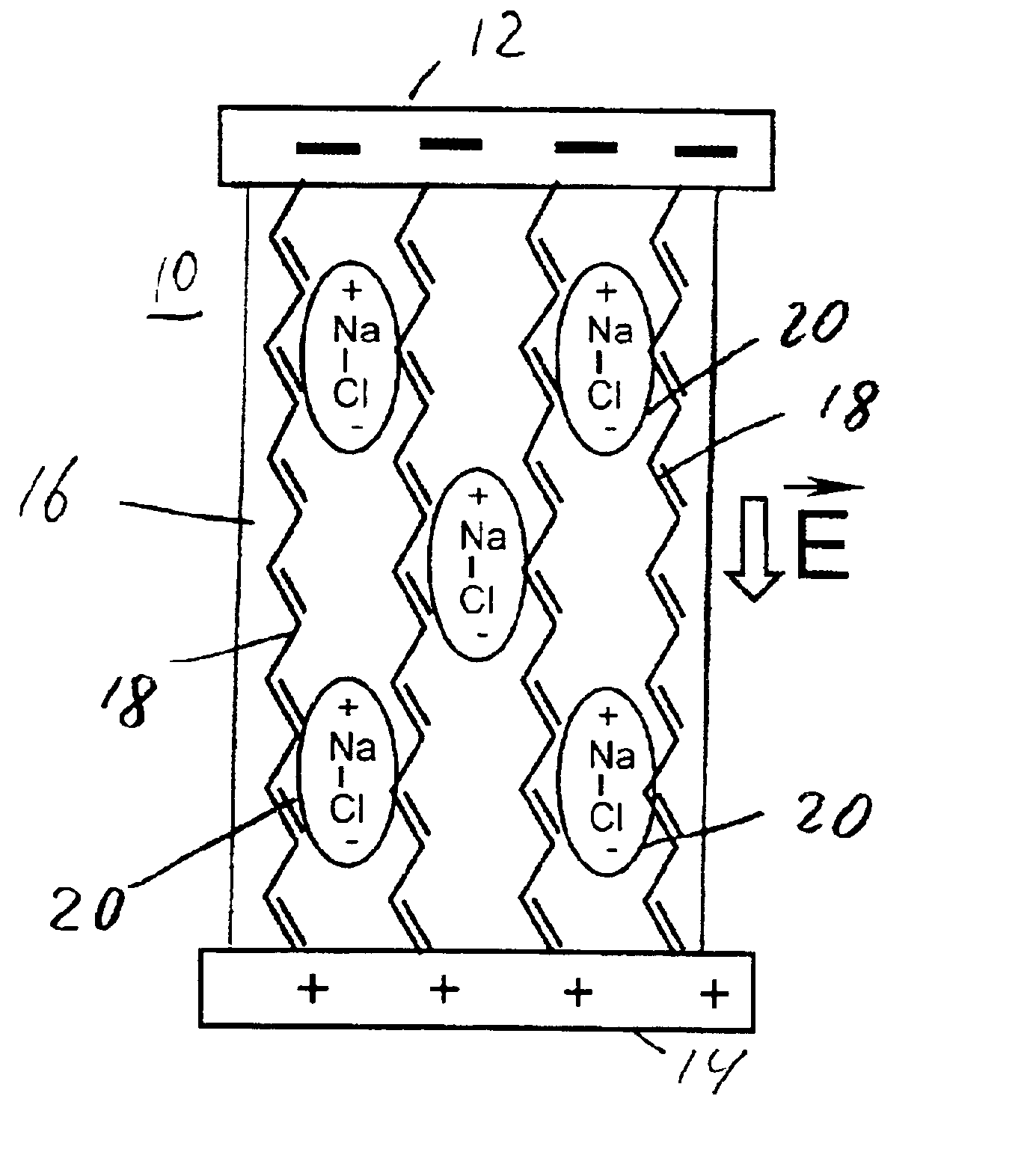
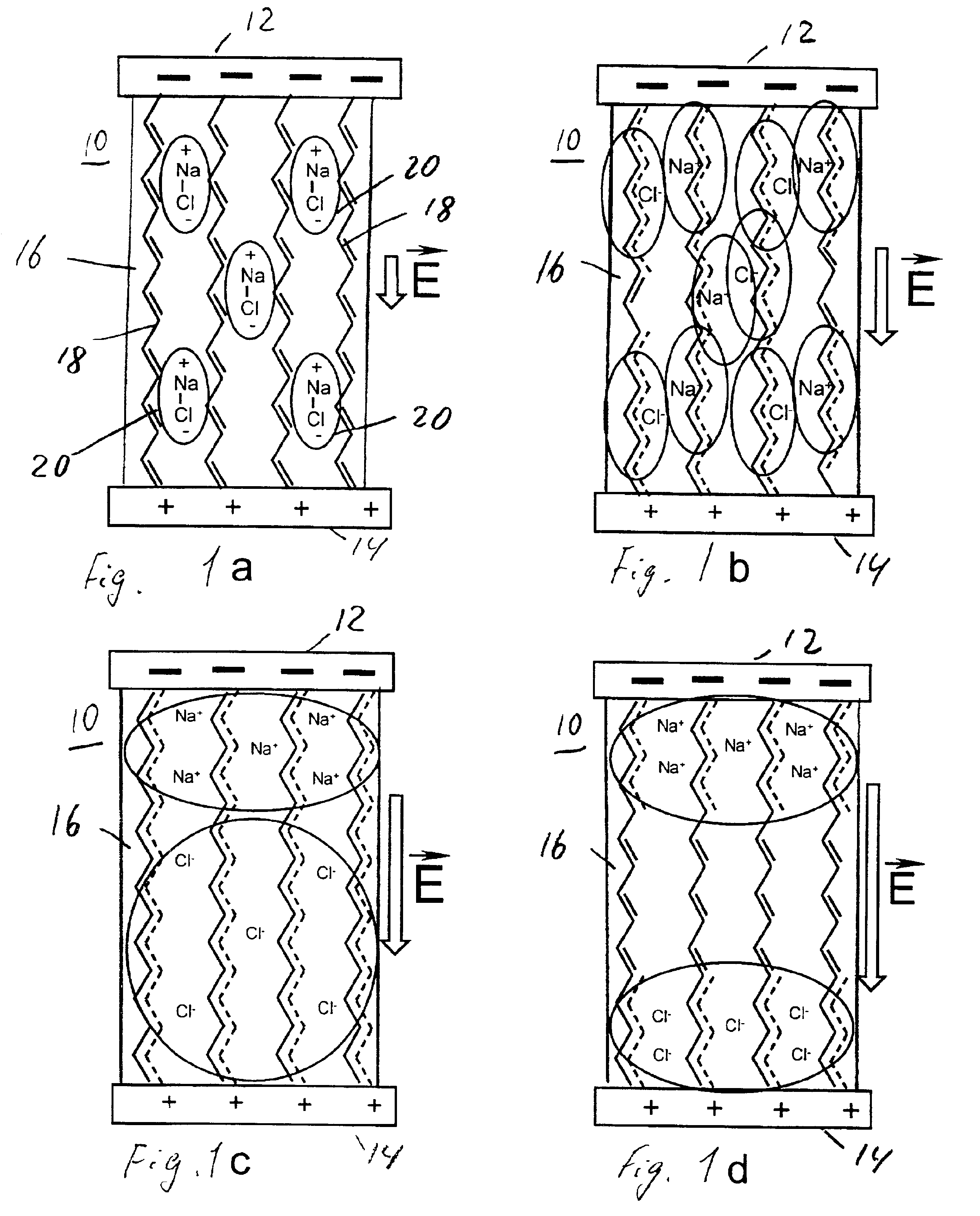
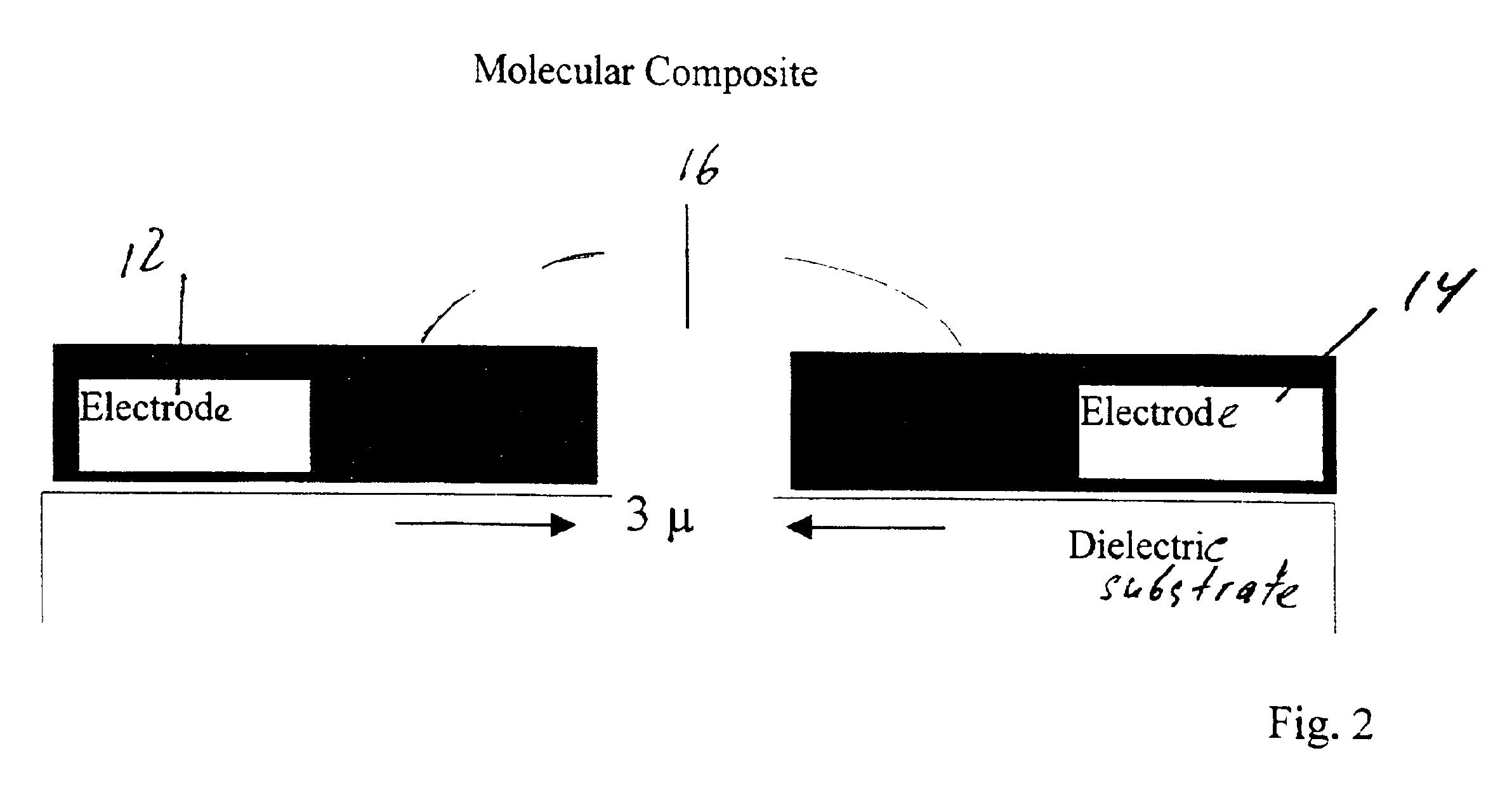
Provided herein is a molecular ensemble that exhibits a reproducible switching and memory effect applicable in practical devices. The material is a composite molecular system that exhibits structural electronic instability in one dimension and enables static and dynamic control over the conductivity of such molecular systems. The mechanism for the memory and switching effect of memory cells relates to the structural electronic instability of one-dimensional molecular systems and is associated with the dissociation of molecules and / or displacement of atoms under influence of an external electrical field.

The development of molecular electronics stimulated the more detailed research of electrophysical characteristics of thin molecular films which offer new physical effects that may result in new technologies for electrical switching and memory applications.

Molecular memory cells can be made of one-dimensional conductive molecular systems exhibiting structural instability. (Peierls-effe...


PUM

PropertyMeasurementUnit
impedanceaaaaaaaaaa
impedanceaaaaaaaaaa
impedanceaaaaaaaaaa

Abstract

A memory cell is provided with a pair of electrodes, and an active layer sandwiched between the electrodes and including a molecular system and ionic complexes distributed in the molecular system. The active layer having a high-impedance state and a low-impedance state switches from the high-impedance state to the low-impedance state when an amplitude of a writing signal exceeds a writing threshold level, to enable writing information into the memory cell. The active layer switches from the low-impedance state to the high-impedance state when an amplitude of an erasing signal having opposite polarity with respect to the writing signal exceeds an erasing threshold level, to enable erasing information from the memory cell.

Description

FIELD OF THE INVENTIONThe invention relates to a molecular memory cell for data storage applications, and, more particularly, to a memory cell made of a composite molecular material.BACKGROUND OF THE INVENTIONComputer data storage, in particular random access memory (RAM) has become an increasingly important component of electronic hardware. There are various distinct types of memory devices, distinguished by their speed and data retention characteristic. Dynamic random access memory (DRAM) is a volatile memory characterized by a destructive read. This means that it is necessary to supply voltage to the memory bits at all times, or the information will disappear. Furthermore, each memory element has associated with it a transistor. Static random access memory (SRAM) stores data in a bistable flip-flop, commonly consisting of cross-coupled inverters. It is called “static” because it will retain a value as long as power is supplied. It is still volatile, i.e. it will lose its contents...

Claims


Application Information

Patent Timeline
Patent Type & Authority Patents(United States)
IPC IPC(8): G11C13/02A01H5/10A23D9/00C11B1/00G11C11/56G11C13/00H01L51/00
CPCA01H5/10H01L51/0595B82Y10/00C11B1/00G11C11/5664G11C13/0009G11C13/0014G11C13/0069A23D9/00G11C2013/0073G11C2013/009G11C2213/13G11C2213/15G11C2213/51G11C2213/77H10K10/701
Inventor KRIEGER, JURI H.YUDANOV, NIKOLAY F.
Owner ADVANCED MICRO DEVICES INC
Why Eureka
Try Eureka