Semiconductor memory device operating with low current consumption

a memory device and semiconductor technology, applied in the direction of information storage, static storage, digital storage, etc., can solve the problems of noise, inability to be neglected, and required data read operation sense current of the order of 10 ma, and achieve accurate reading and low current consumption

Inactive Publication Date: 2005-03-29
RENESAS ELECTRONICS CORP
View PDF6 Cites 81 Cited by
  • Summary
  • Abstract
  • Description
  • Claims
  • Application Information

AI Technical Summary

Benefits of technology

Accordingly, an object of the invention is to provide a nonvolatile semiconductor memory device, in which data can be accurately read with a low current consumption.
Another object of the invention is to provide a semiconductor memory device, in which a leakage current during the standby is reduced without impairing a high speed operation.
A voltage applied to a power supply node of a circuit for driving the signal line connected to a memory cell is changed in accordance with the operation mode in the invention of the first aspect. Thus, a leakage current during the standby can be reduced without lowering a driving capability of the signal line drive circuit.
The substrate region of each circuit is isolated so that propagation of noises is limited within each substrate region, and a noise margin is improved in the invention of the third aspect. Each memory block can be driven in a block basis so that the current consumption can be further reduced.
By adjusting a back gate voltage in accordance with the operation mode, it is possible to increase the driving power of the transistor in operation without increasing the size of the transistor so that the memory cell can be selected quickly without increasing an area of the circuit. Therefore, it is possible to achieve the semiconductor memory device, which occupies only a small area and can operate fast with a low current consumption.

Problems solved by technology

GMR element has a resistance changing rate ranging from 6 to 8%, and has a disadvantage that a sense current of the order of 10 mA is required in a data read operation.
Therefore, if characteristics of the access transistors vary, read current differ among the access transistors, and noises caused by these variations cannot be neglected.
Therefore, a sufficient signal-to-noise ratio cannot be achieved in the TMR element, for which a sense current of 10 μA can provide a memory cell read voltage of 25 mV.
Therefore, it is difficult to remove completely the offset in output voltage of the memory cell, which is caused by variations in characteristics of the access transistors.
Accordingly, if variation is present in film thickness of the tunnel film, this increases difference in resistance value of the tunneling film between the selected memory cell and the dummy cell, so that differential input voltages to the differential amplifier may become insufficient or inverted.
Therefore, the memory cell data cannot possibly be accurately detected.
Accordingly, the leakage currents in this drive circuit group increase the current consumption during the standby, so that a specification requirement of an ultra low standby current, which is required for application such as portable equipment, cannot be satisfied, and the application range is restricted.
In this case, however, the responsivility of the MOS transistor is deteriorated, and a drive current also decreases, if the transistor size is unchanged.
Accordingly, if the absolute value of the threshold voltage is made great, it is impossible to reduce the transistor sizes for a faster operation, and thus the device shrinking is impeded.

Method used


Image

  • Semiconductor memory device operating with low current consumption
  • Semiconductor memory device operating with low current consumption
  • Semiconductor memory device operating with low current consumption

Examples


first embodiment

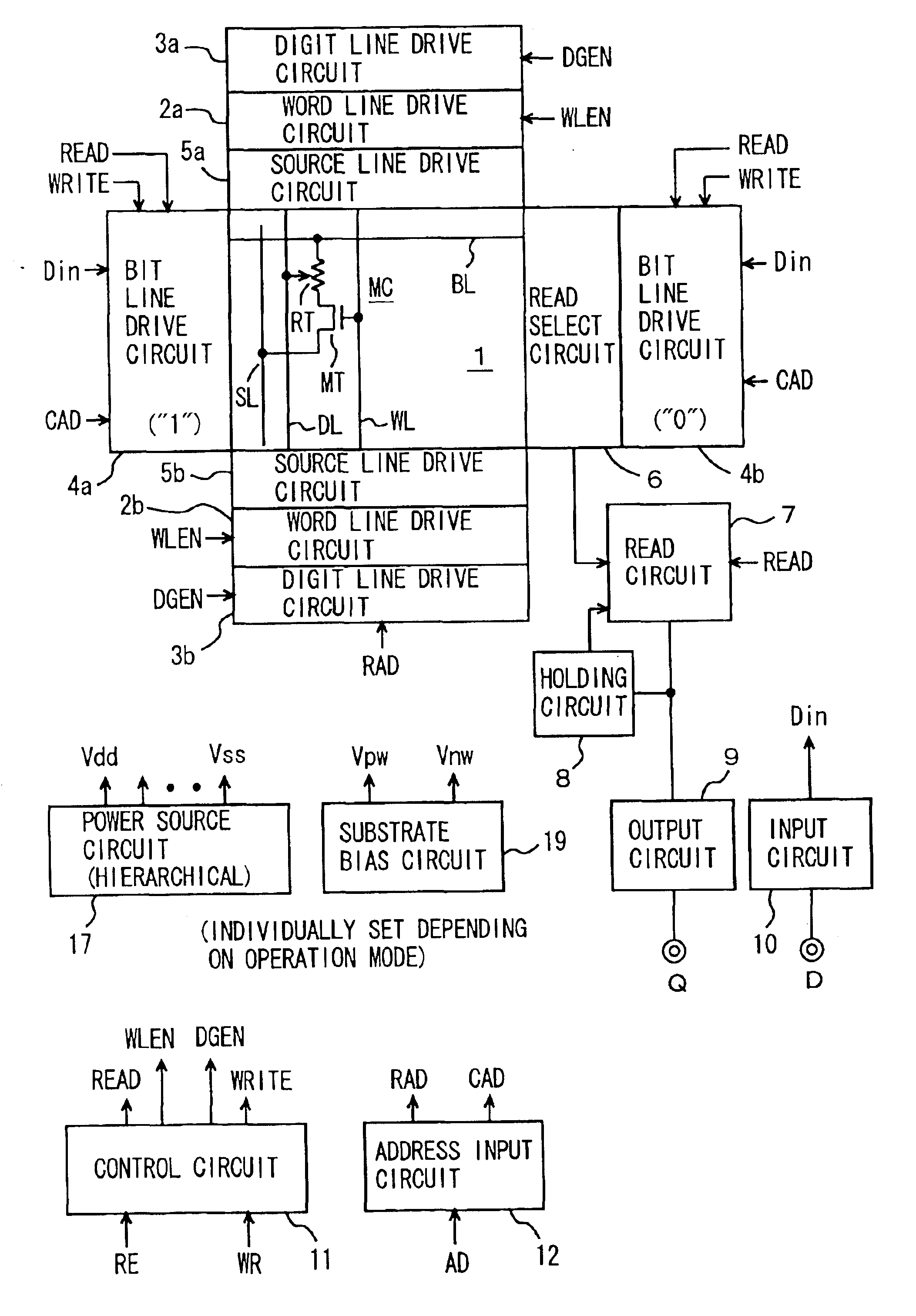
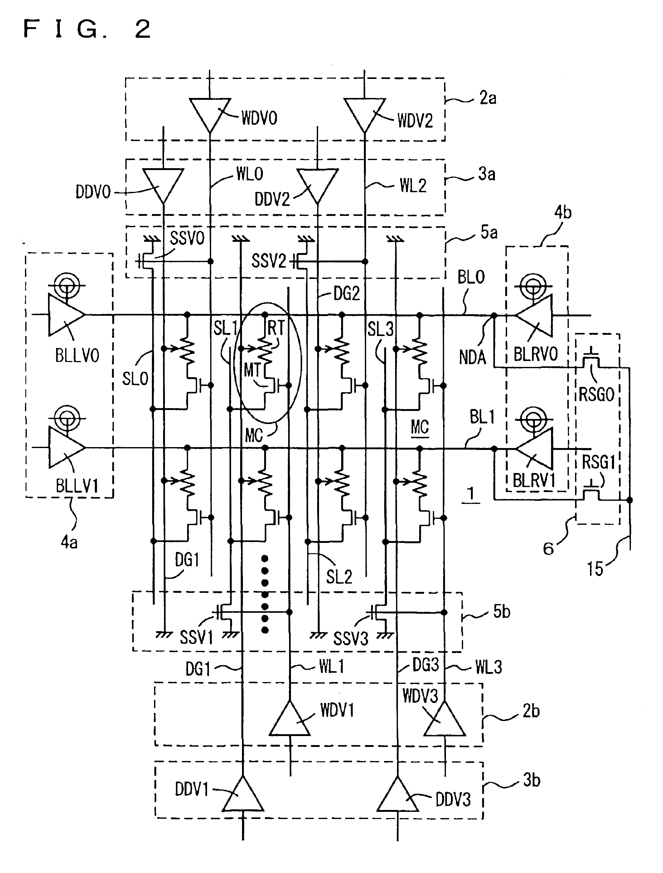
FIG. 1 schematically shows a whole structure of a nonvolatile semiconductor memory device according to a first embodiment of the invention. In FIG. 1, the nonvolatile semiconductor memory device includes a memory cell array 1 having memory cells MC arranged in rows and columns. Memory cell MC includes a variable resistance element (TMR element) RT having a resistance value variable in accordance with storage data, and an access transistor MT for selecting resistance element RT for connection to a source line SL in accordance with a signal on a word line WL. Access transistor MT is formed of an N-channel MOS transistor.

A write word line, a read word line, a write bit line and a read bit line are arranged corresponding to memory cell MC. For the sake of simplicity, the write bit line will be merely referred to as “bit line BL”, and the write word line will be referred to as “digit line DL”, the read word line referred to as “word line WL”, and the read bit line as “source line SL” in ...


PUM


Abstract

In a resistance value variable memory, substrate voltages and / or substrate biases of a digit line drive circuit, a word line drive circuit and a bit line drive circuit for a memory cell array are changed in accordance with an operation mode. A driving power on signal lines connected to memory cells can be increased, and a leakage current during standby can be reduced without increasing a circuit layout area.

Description

BACKGROUND OF THE INVENTION1. Field of the InventionThe present invention generally relates to a semiconductor memory device, and particularly to a nonvolatile semiconductor memory device, in which memory cells include resistance elements having resistance values varying in accordance with storage data. More particularly, the invention relates to a structure for reducing a current consumption of a semiconductor device, particularly a nonvolatile semiconductor memory device.2. Description of the Background ArtSuch a memory device is known that a variable resistance element is utilized in a memory cell, and data is nonvolatilely stored by a resistance value of this variable resistance element. A phase change memory and a Magnetic Random Access Memory (MRAM) are known as the memory of such type.In the phase change memory, a material such as polycrystalline silicon is set to an amorphous state or a crystalline state in accordance with data to be stored. Since the amorphous state and the...

Claims


Application Information

Patent Timeline
Patent Type & Authority Patents(United States)
IPC IPC(8): G11C11/15G11C11/02
CPCG11C11/15
Inventor OOISHI, TSUKASA
Owner RENESAS ELECTRONICS CORP
Why Eureka
Try Eureka