Substrate processing method and substrate processing apparatus

a substrate processing and substrate technology, applied in the direction of photosensitive material processing, transportation and packaging, coatings, etc., can solve the problem that the air down flow described above is not able to remove the impurities of molecule level, and achieve the effect of improving the uniformity of line width

Inactive Publication Date: 2005-04-05
TOKYO ELECTRON LTD
View PDF12 Cites 13 Cited by
  • Summary
  • Abstract
  • Description
  • Claims
  • Application Information

AI Technical Summary

Benefits of technology

Considering the above-described circumstances, an object of the present invention is to provide a substrate processing method and substr...

Problems solved by technology

The down flow of the air described above is n...

Method used


Image

  • Substrate processing method and substrate processing apparatus
  • Substrate processing method and substrate processing apparatus
  • Substrate processing method and substrate processing apparatus

Examples


fifth embodiment

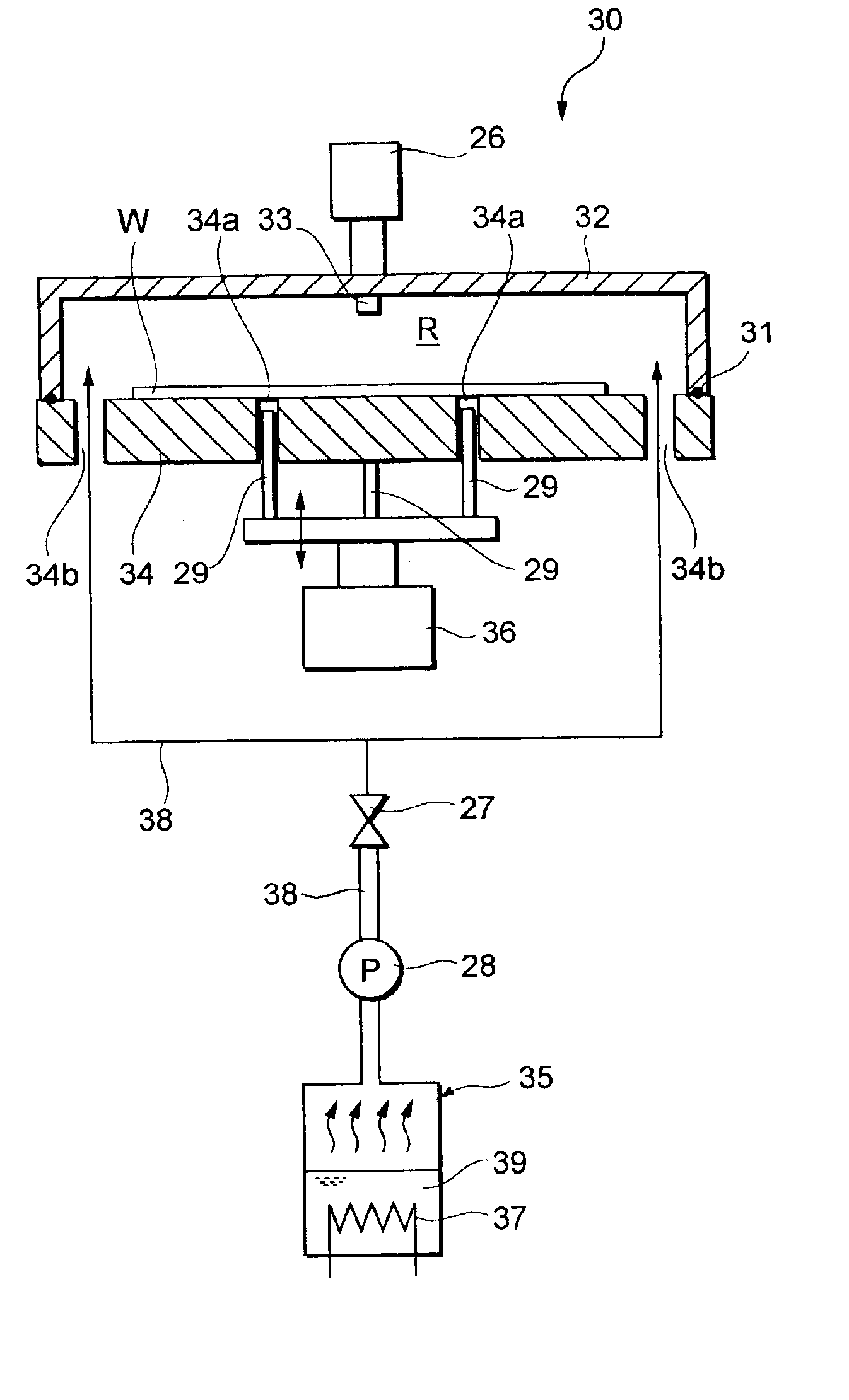
FIG. 11 is a sectional view showing a vapor processing unit according to the present invention. Incidentally in FIG. 11, the same numerals and symbols will be used to designate the same components as those in FIG. 4, and the explanation thereof will be omitted.

A vapor processing unit 70 has an increasing and reducing pressure apparatus 72. A pipe 75 is connected between the increasing and reducing pressure apparatus 72 and an air introduction and exit port 73 provided on the lid 32 and the increasing and reducing pressure apparatus 72 controls the pressure inside the processing chamber R under control of a controller 71. As the increasing and reducing pressure apparatus 72, a vacuum pump and the like which introduces air into and sucks out the air out of the processing chamber R can be used.

A pressure measuring sensor 74 is attached, for example, to the inside of the lid 32. The pressure measuring sensor 74 detects the pressure inside the processing chamber R and the controller 71 c...

sixth embodiment

FIG. 12 is a sectional view showing a vapor processing unit according to the present invention. Incidentally, in FIG. 12, the same numerals and symbols will be used to designate the same components as those in FIG. 4, and the explanation thereof will be omitted.

In a vapor processing unit 80, a moisture film thickness measuring apparatus 81 is attached inside the lid 32. The moisture film thickness measuring apparatus 81 measures the film thickness of the vapor adhered to the surface of the wafer W, after the wafer W is exposed to the vapor. As the moisture film thickness measuring apparatus 81, for example, an apparatus using a principle of measuring the film thickness with light interference can be used.

A controller 82 controls switching of the pump 28 corresponding to the measurement result of the moisture film thickness measuring apparatus 81, therefore, the amount of vapor supplied into the processing chamber R can be controlled.

One example of an operation of the vapor processin...


PUM

PropertyMeasurementUnit
Temperatureaaaaaaaaaa
Thicknessaaaaaaaaaa
Pressureaaaaaaaaaa

Abstract

The wafer coated with the resist is deliberately placed in the vapor before being transferred to an aligner that exposes the resist on the wafer, the vapor, for example, the moisture, uniformly adheres onto the resist on the wafer. As a result, the substrate can uniformly be exposed in the following exposing process, and the uniformity of the line width and the like can be improved.

Description

BACKGROUND OF THE INVENTION1. Field of the InventionThe present invention relates to a substrate processing apparatus for coating a semiconductor wafer with a resist and developing thereof in a fabrication of semiconductor device. In detail, the invention relates to a substrate processing apparatus that controls the atmosphere of the processing environment of the substrate.2. Description of the Related ArtIn a process of photolithography in the semiconductor device fabrication, the surface of a semiconductor wafer (hereinafter referred to as “a wafer”) is coated with a photo-resist, exposing a mask pattern on the resist, then developing thereof, forming a resist pattern on the wafer surface. The resist coating and development are performed in an integrated coating and developing processing apparatus including a thermal processing apparatus such as a heating processing apparatus or a cooling processing apparatus. The coating and developing apparatus is connected to the aligner throug...

Claims


Application Information

Patent Timeline
IPC IPC(8): H01L21/00G03F7/38H01L21/027H01L21/677
CPCH01L21/67178H01L21/67751H01L21/67748
Inventor MATSUI, HIDEFUMIKITANO, JUNICHI
Owner TOKYO ELECTRON LTD
Why Eureka
Try Eureka