Surface protecting adhesive film for semiconductor wafer and processing method for semiconductor wafer using said adhesive film

a technology of adhesive film and semiconductor wafer, which is applied in the direction of semiconductor devices, semiconductor/solid-state device details, electrical devices, etc., can solve the problems of serious problems, layered semiconductor wafer may have a significant degree of warpage deformation, processing may come to a halt, etc., and achieves the effect of preventing damage to the wafer, straightening or avoiding warpage of semiconductor wafers, and easy peeling

Inactive Publication Date: 2005-04-12
MITSUI CHEM TOHCELLO INC
View PDF2 Cites 13 Cited by
  • Summary
  • Abstract
  • Description
  • Claims
  • Application Information

AI Technical Summary

Benefits of technology

The object of the present invention is, in view of the above problems, to provide an adhesive film for protecting the surface of a semiconductor wafer which makes it possible to straighten or avoid warpage of semiconductor wafers caused by the residual stress of circuit protection films thereof as well as to be easily peeled therefrom without damaging wafers even if the thickness of wafers is reduced down to 150 μm or less in the grinding process of the non-circuit-formed surface of semiconductor wafers, and a method of processing the non-circuit-formed surface of semiconductor wafers using the same.
In the back grinding process for a semiconductor wafer, it is possible by using the adhesive film for protecting the surface of a semiconductor wafer concerning the present invention to restrain the substrate film from elongation when adhering said adhesive film for protecting the surface of a semiconductor wafer to the circuit-formed surface thereof in order to straighten or avoid the wafer's warpage caused by residual stress of the circuit protection film for a semiconductor wafer, even if a wafer of which circuits are protected by a protection film is reduced in its thickness to 150 μm or less. Meanwhile, the substrate film of said adhesive film for protecting the surface of a semiconductor wafer expands moderately by coolant poured in the grinding process for the non-circuit-formed surface of a semiconductor wafer, washing water for the adhesive surface of the film and so on, making it possible to straighten or avoid warpage of semiconductor wafers so that the damage of wafers can be prevented. Also, the adhesive film for protecting the surface of a semiconductor wafer concerning the present invention can be easily peeled off from the circuit-formed surface of a semiconductor wafer without damaging wafers by heating because the elastic modulus of the substrate film decreases by heating.
One effect of the present invention is, by using the adhesive film for protecting the surface of a semiconductor wafer concerning the present invention, the elongation of the substrate film can be prevented which may occur in adhering the adhesive film for protecting the surface of a semiconductor wafer on the circuit-formed surface of a semiconductor wafer, to straighten or prevent the warpage of wafers caused by the residual stress of a circuit protection film for semiconductor wafers even if the thickness of a wafer of which circuits are protected by a protection film is reduced down to 150 μm or less in the back grinding process for a semiconductor wafer. Another effect is that the damage of wafers can be prevented by straightening and preventing the warpage of semiconductor wafers because the substrate film of the adhesive film for protecting the surface of a semiconductor wafer is appropriately expanded by cooling water which is poured in grinding the circuit-formed surface of a semiconductor wafer or washing water for the surface of the adhesive film, etc. A further effect is that the adhesive film for protecting the surface of a semiconductor wafer concerning the present invention can be easily peeled off from the circuit-formed surface of a semiconductor wafer without damaging the wafer by heating it in peeling, because the elastic modulus of the substrate film decreases.

Problems solved by technology

However, such a thin-layered semiconductor wafer may have a significant degree of warpage deformation because of its deteriorating rigidity, which becomes a manufacturing problem.
If the warpage deformation of the wafer is significant during these processes, some of the processing may come to a halt because the wafer is damaged or because the robot can not convey the wafer, and so on.
Also in the peeling process of the adhesive film for protecting the surface of a semiconductor wafer, serious problem such as the damage of wafers may occur because of flattening the wafer by force in fixing it to the “chuck table” in the peeling machine.
A thinning-processed semiconductor wafer may cause a warpage deformation.
Generally speaking, adhesive film for protecting the surface of a semiconductor wafer using a stretchy, flexible substrate film tends to cause a big residual stress, resulting in an easy occurrence of warpage in semiconductor wafers.
Especially, if the polyimide group protection film is thick in the process of reducing the thickness of a semiconductor wafer, the warpage of the wafer increases by the residual stress of said polyimide group protection film, which may result in serious problems such as the halt of manufacturing processes caused by the damage of wafers or by incapability of conveyance by robots and so on.
Though the adhesive film for protecting the surface of a semiconductor wafer using the substrate film with high percentage of stress relaxation disclosed in Japanese Laid-open patent Publication No.2000-150432 is effective to decrease the residual stress applied in adhering it to the surface of semiconductor wafers, it can not avoid any warpage of the semiconductor wafers which is caused by residual stress of circuit protection films.
The adhesive film for protecting the surface of a semiconductor wafer using substrate film with high linear elastic modulus disclosed in Japanese Laid-open Patent Publication No.2000-212524, on the other hand, is effective to straighten the warpage of semiconductor wafers, but it is difficult to peel from the surface thereof.

Method used


Image

  • Surface protecting adhesive film for semiconductor wafer and processing method for semiconductor wafer using said adhesive film
  • Surface protecting adhesive film for semiconductor wafer and processing method for semiconductor wafer using said adhesive film

Examples


example 1

4. Example 1 of Preparing Adhesive Agent Coating Solution

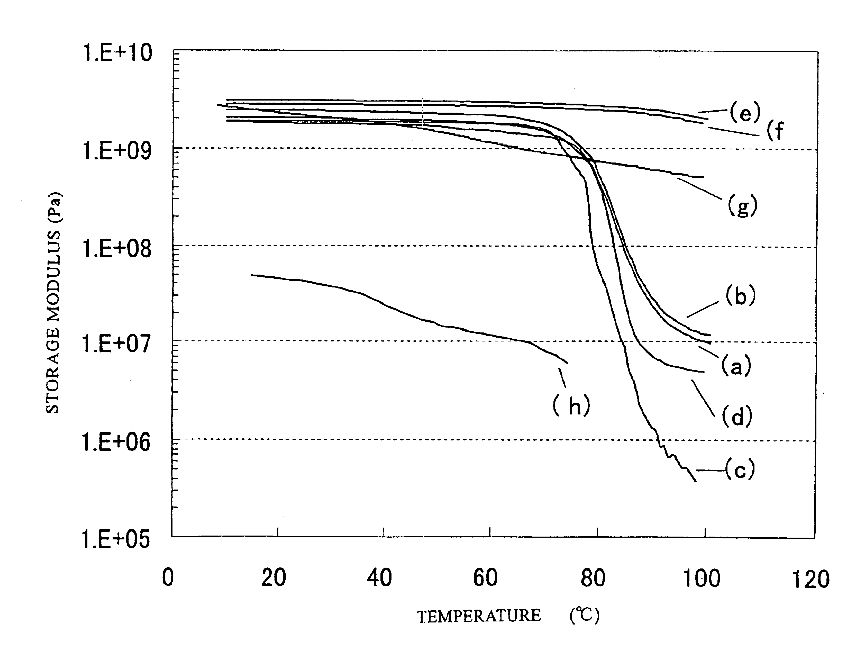
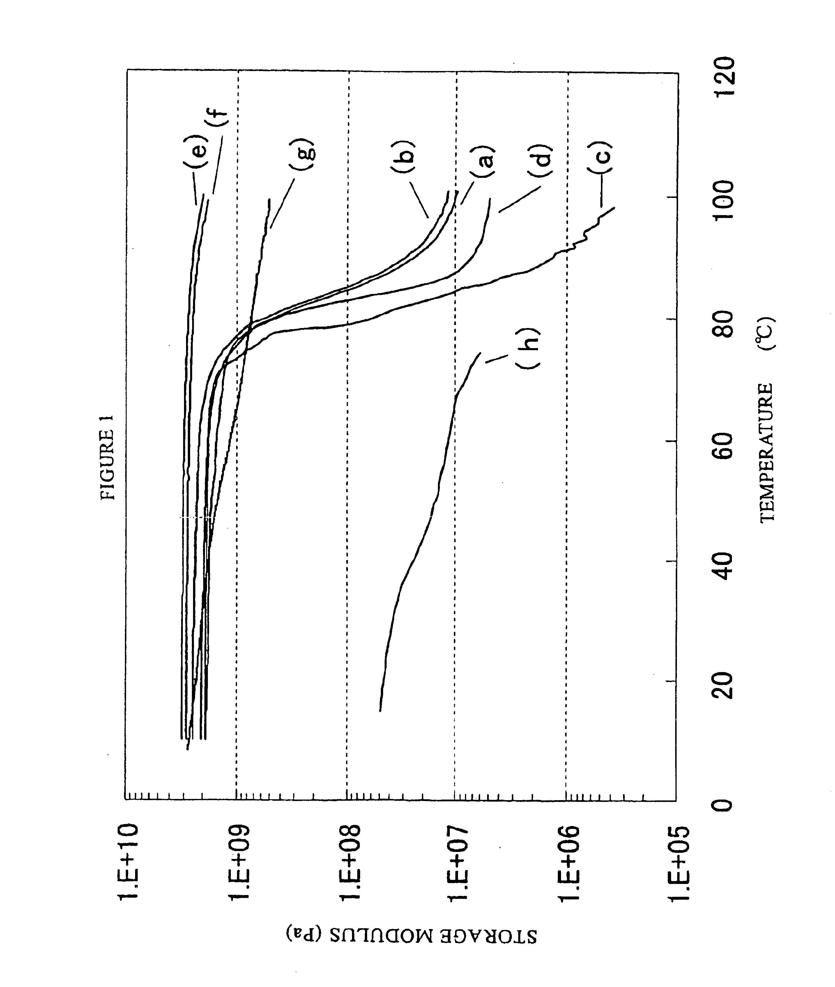
Emulsion polymerization was conducted for nine hours by adding deionized water 150 parts by weight, 4,4′-azobis(4-cyano valeric acid) [manufactured by Otsuka Chemical Co., Ltd, trade name: ACVA] 0.5 parts by weight as polymerization initiators, butyl acrylate 52.25 parts by weight, ethyl methacrylate 25 parts by weight, 2-hydroxyethyl methacrylate 15 parts by weight, methacrylic acid 6 parts by weight, acryl amide 1 part by weight, and ammonium salt of polyoxyethylene nonylphenyl ether sulfate (the average number of added moles of ethyleneoxide:about 20) in which the benzene ring is introduced by polymeric 1-propenyl group [manufactured by Dai-ichi Kogyo Seiyaku Co, Ltd., trade name: AQUALON HS-20] 0.75 parts by weight as a water soluble comonomer into a polymerization reactor, keeping stirring at temperature 70° C. to obtain an acrylic resin water emulsion. Then it was neutralized with ammonia water of 14 weight percent, to o...


PUM

PropertyMeasurementUnit
RHaaaaaaaaaa
total thicknessaaaaaaaaaa
thicknessaaaaaaaaaa

Abstract

An adhesive film for protecting the surface of a semiconductor wafer wherein the adhesive layer is formed on one surface of a substrate film, the substrate film comprising at least one layer which satisfies the following requisites (A) and at least one of (B) or (C):requisite (A): high elastic modulus properties in which the storage modulus is 1×10⁹ Pa to 1×10¹⁰ Pa under the total temperature range of from 18 to 50° C.requisite (B): high elastic modulus properties in which the storage modulus within at least part of the temperature range of from 50 to 90° C. is not more than 1×10⁸ Pa.requisite (C): high elastic modulus properties with expansibility by water absorption in which the size-changing ratio by absorbing water for four hours is 0.05 to 0.5% at 23° C. and 90% RH.

Description

FIELD OF THE INVENTIONThis invention relates to an adhesive film for protecting the surface of a semiconductor wafer and method of processing the non-circuit-formed surface of a semiconductor wafer using said adhesive film for protecting the surface of a semiconductor wafer. More specifically, it relates to an adhesive film for protecting the surface of a semiconductor wafer which is used by adhering to the surface of a semiconductor wafer made of silicon and gallium arsenide (GaAs) and so on wherein an circuit is formed in processing the other surface of said wafer, and method of processing the non-circuit-formed surface of the semiconductor wafer using the same.More specifically, it relates to an adhesive film for protecting the surface of a semiconductor wafer which is preferable for damage protection and improvement of productivity of the semiconductor wafer in the manufacturing process of a thin-layered semiconductor chip, especially in the non-circuit-formed surface processing...

Claims


Application Information

Patent Timeline
Patent Type & Authority Patents(United States)
IPC IPC(8): C09J7/02H01L21/68
CPCC09J7/0264H01L21/6836H01L2221/68327C09J2203/326C09J7/22H01L21/304
Inventor FUKUMOTO, HIDEKIKOSHIMIZU, TAKANOBUKATAOKA, MAKOTOSAIMOTO, YOSHIHISA
Owner MITSUI CHEM TOHCELLO INC
Why Eureka
Try Eureka