Delay circuit, semiconductor integrated circuit device containing a delay circuit and delay method

a delay circuit and semiconductor technology, applied in pulse manipulation, pulse technique, instruments, etc., can solve the problems of increasing the adjustment accuracy of the delay circuit for timing adjustment, increasing the operating leeway, and becoming extremely shor

Inactive Publication Date: 2005-04-12
SOCIONEXT INC
View PDF9 Cites 46 Cited by
  • Summary
  • Abstract
  • Description
  • Claims
  • Application Information

AI Technical Summary

Benefits of technology

The present invention was conceived in order to solve the above problems in the related technology and it is an object thereof to provide a delay circuit, a semiconductor integrated circuit device containing the delay circuit, and a delay method, that enable a delay signal having a predetermined delay time and a delay pulse having a predetermined time width to be accurately and appropriately generated by accurately adding a delay time where appropriate to a propagated signal from the input of the signal without causing any waveform deformation or parasitic delay caused by parasitic elements.

Problems solved by technology

Due to the increased speed of the CPU and system LSI and the like, the operational leeway in the mutual transition timing between signals in the internal critical paths has become extremely short and the adjustment time steps and the adjustment accuracy of the delay circuit for the timing adjustment are becoming more and more exacting.
In addition, because the area on a chip allocated to be taken up by the delay circuit 1000 is limited, it is not possible to make the size of the transistor sufficiently large.
Moreover, because the parasitic resistance and capacitance vary widely due to inconsistencies in the manufacturing of the semiconductor integrated circuit devices, the delay amount and the like of these parasitic elements are also varied.
Because this is a time that is approximately ten times the size of the unit delay time, a delay from the parasitic element of approximately ten times the adjustment value of the delay time is added to the adjustment value of the unit delay time causing the problem that it is not possible to accurately adjust the delay amount.
In particular, as adjustment of the delay amount in more minute time step will henceforth be required in response to the ever increasing speed of semiconductor integrated circuit devices, it is going to be difficult to accurately perform the delay adjustment.
Moreover, circuit operation is necessary in short pulses, however, the concern exists that the short pulses will become flattened and disappear due to the rounding of the waveform caused by the parasitic delay elements.
In this case, the problem arises that the semiconductor integrated circuit device might cause operational malfunctions.
However, the problem with this is that while the delay—rounding effect caused by the parasitic elements becomes greater the more stages there are in the delay section 100, the increase in the drive capacity of the inverter gates 102 through 402 becomes limited by the restrictions of the allowable surface area on the chip, creating the concern that it will become even more difficult to respond to the demands for adjustment of the delay amount in even more minute time step to go with the increased speeds of the semiconductor integrated circuit devices.
Therefore, in the delay circuit 2000 having a multi stage structure, because more of the terminals N11 through N41 are needed and a large area is required for the wiring on the chip surface, the problem arises that the further integration of the semiconductor integrated circuit device is held back.
However, because the dimensions of the logic circuit become more complex as the more terminals N11 through N41 are needed as signal paths in the multi stage structure delay circuit 2000 requiring a large area of the chip surface, the problem arises that the further integration of the semiconductor integrated circuit device is held back.
Accordingly, the problem arises in the delay circuit 3000 having a multi stage structure that, as a result of the drive capacity of the inverter gate 800 becoming more and more insufficient as the capacitance load of the terminal N800 increases, the possibility exists that short pulse waveform will become ragged.
Therefore, the drive capacity is unbalanced because the drive capacity of the sink drive is weaker than the drive capacity of the source drive.
The problem is thus that the possibility exists that the short pulse propagation needed as the speed of the semiconductor integrated circuit device increases may not be obtainable.
However, such measures create the problem that they require a large portion of the chip surface area thereby preventing further advances in the level of integration of the semiconductor integrated circuit device.
In addition, any increase in the size of the transistor in itself means that there is an increase in the parasitic capacitance and gives rise to the problem that a greater number of stages in the structure of the delay circuit 3000 and faster operation are not able to be achieved.

Method used


Image

  • Delay circuit, semiconductor integrated circuit device containing a delay circuit and delay method
  • Delay circuit, semiconductor integrated circuit device containing a delay circuit and delay method
  • Delay circuit, semiconductor integrated circuit device containing a delay circuit and delay method

Examples


first embodiment

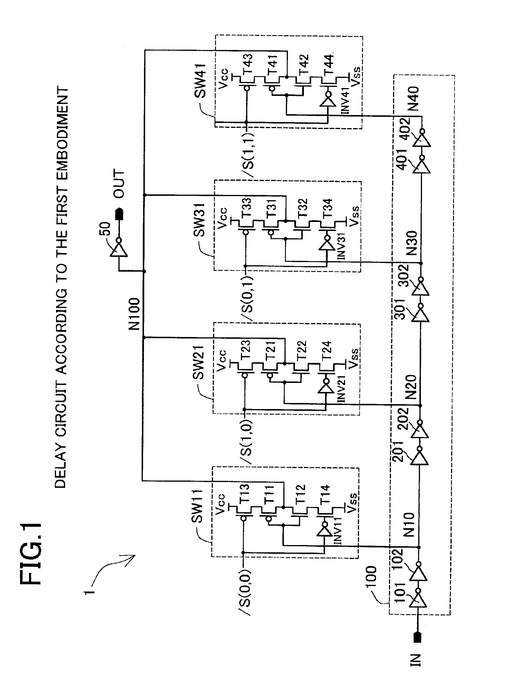
A delay circuit 1 of a first embodiment shown in FIG. 1 is provided with selecting switch sections (selecting switch means) SW11, SW21, SW31, and SW41 instead of the selecting switch sections SW110 through SW410 of the first delay circuit 1000 of the related technology (see FIG. 8). Unlike the selecting switch sections SW110 through SW410 of the first delay circuit 1000 of the related technology, because a logic inversion function is included in the selecting switch sections (selecting switch means) SW11 through SW41, the output buffer circuit 500 is changed from a two stage structure formed from the inverter gates 501 and 502 to an output buffer circuit 50 that has a one stage inverter gate structure.

The selecting switch section (selecting switch means) SW11 is formed from a buffer section (buffer means) and a selecting section (selecting section means). The buffer section (buffer means) comprises an output terminal N100 that connects together the drain terminals of the PMOS transi...

second embodiment

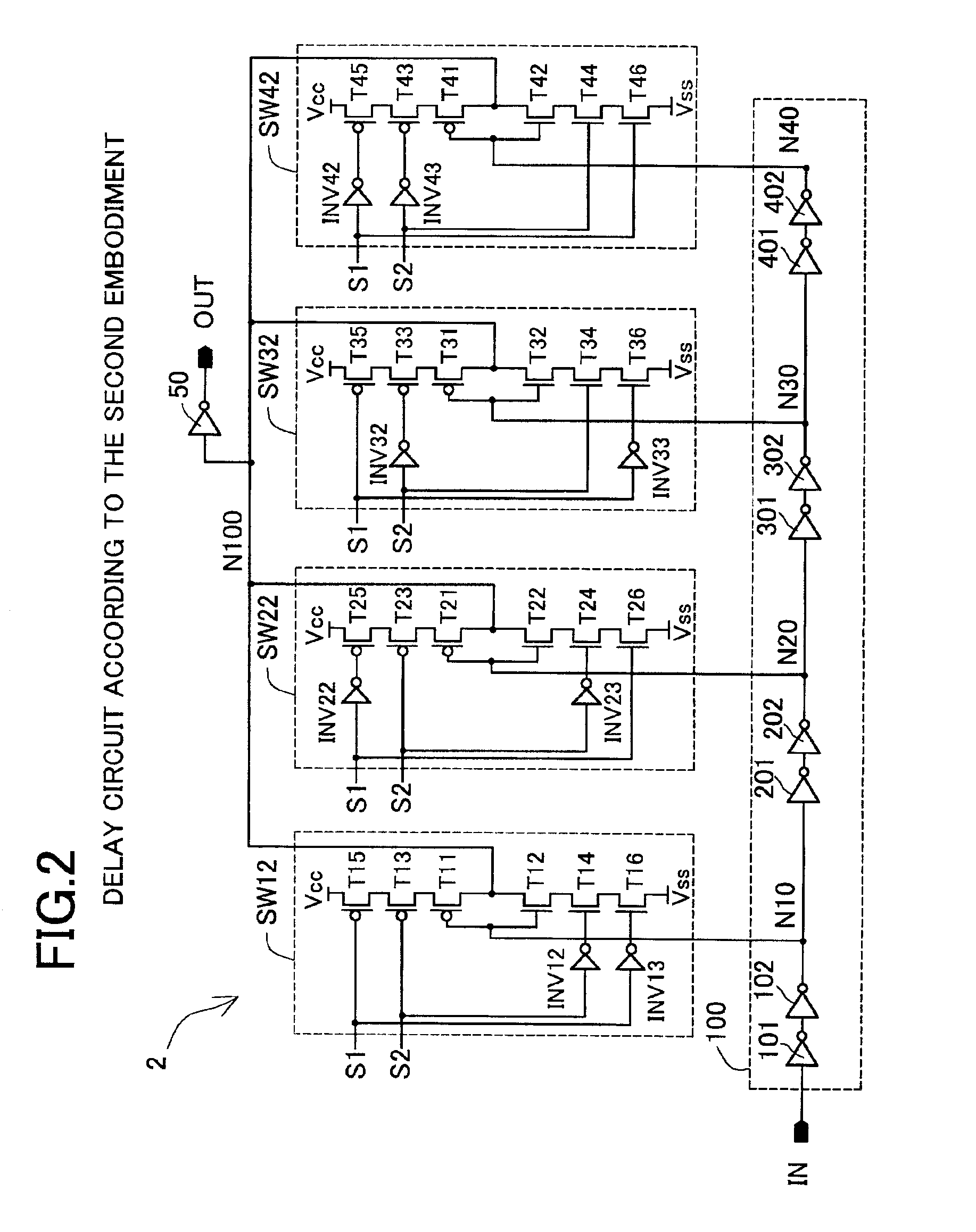
In the delay circuit 2 of the second embodiment, the structure described is one in which in order to ensure the drive capacity of the MOS transistors T13, T14, T15, and T16 through T43, T44, T45, and T46 forming the selecting sections (selecting section means) in the selecting switch sections (selecting switch means) SW12 through SW42, the inverter gates INV12 and INV13 through INV42 and INV43 for supplying inverted signals of the control signals S1 and S2 are provided for each transistor, however, when the drive capacity of the inverter gate is sufficient, it is also possible for the inverted signals to be supplied from one inverter gate.

As has been described above, the delay circuit 2 of the second embodiment is an example of when the delay path in the delay section 100 is established using the logic combinations of control signals S1 and S2, which are two composite control signals. Instead of the PMOS transistors T13 through T43 and the NMOS transistors T14 through T44, there are...

fourth embodiment

In the delay circuit 4 of the fourth embodiment as described above, the PMOS and NMOS transistors T11 through T41 and T12 through T42 connected to the power supply voltage Vcc and the ground potential Vss are connected to the output terminals N100 of the selecting switch sections (selecting switch means) SW13 through SW43 via the PMOS and NMOS transistors T13 through T43 and T14 through T44. Because the PMOS and NMOS transistors T13 through T43 and T14 through T44 are inserted between the PMOS and NMOS transistors T11 through T41 and T12 through T42 and the output terminals N100, when the PMOS and NMOS transistors T11 through T41 and T12 through T42 are activated, the effects from the level transition of the propagated signal input into the gate terminal do not appear at the output terminals N100.

Note that the remainder of the basic operation and effects are the same as those of the first embodiment.

A delay circuit 5 of the fifth embodiment shown in FIG. 5 is structured such that, i...


PUM


Abstract

A delay circuit including a delay section having two or more predetermined delay stages is disclosed. Each predetermined delay stage adds a predetermined delay time to an input signal. The delay circuit also includes selecting switch sections. At least one of the selecting switch sections includes: a buffer section for receiving a delayed input signal from one of the delay stages and a selecting section means directly connected to the buffer section for activating the buffer section to establish a delay path, wherein an output signal from the delay path has a desired delay time.

Description

BACKGROUND OF THE INVENTION1. Field of the InventionThe present invention relates to a delay circuit, a semiconductor integrated circuit device containing a delay circuit and a delay method that enable signal propagation delay time to be adjusted in a semiconductor integrated circuit device without being affected by parasitic elements.2. Description of the Related ArtRecent years have seen even further progress in the increasing speed of semiconductor integrated circuit devices. Due to the increased speed of the CPU and system LSI and the like, the operational leeway in the mutual transition timing between signals in the internal critical paths has become extremely short and the adjustment time steps and the adjustment accuracy of the delay circuit for the timing adjustment are becoming more and more exacting. Moreover, as a result of the increasing speed of the CPU and system LSI etc., there is also a need for a synchronous semiconductor memory device such as is typified by synchro...

Claims


Application Information

Patent Timeline
Patent Type & Authority Patents(United States)
IPC IPC(8): H03K5/13H03K5/00G11C8/00G11C11/4076H03K5/14
CPCH03K5/133H03K2005/00065G11C8/00
Inventor KOMURA, KAZUFUMIKAWAMOTO, SATORU
Owner SOCIONEXT INC
Why Eureka
Try Eureka