Method and apparatus for routing harmonics in a plasma to ground within a plasma enhanced semiconductor wafer processing chamber

a technology of enhanced semiconductor wafers and processing chambers, which is applied in the direction of liquid/fluent solid measurements, instruments, volume measurement, etc., can solve the problems of ineffective etching of certain portions of the wafers, non-uniform plasma processing of the wafers, and destruction of devices, so as to improve the uniformity of plasma processing, suppress the effect of harmonic energy, and enhance the processing chamber.

Inactive Publication Date: 2005-04-12
APPLIED MATERIALS INC
View PDF4 Cites 24 Cited by
  • Summary
  • Abstract
  • Description
  • Claims
  • Application Information

AI Technical Summary

Benefits of technology

The present invention is a method and apparatus for routing harmonic energy in a plasma to ground within a plasma enhanced semiconductor wafer processing chamber. The invention uses a model of the chamber and its RF drive electronics to determine coupling pathways for the applied RF power and the associated harmonic energy. From this model, the placement and design of a harmonic shunt can be determined to route the harmonic energy to ground and suppress the effect of the harmonic energy upon the plasma processing. In one embodiment of the invention, the circuit for routing the harmonics in a plasma reactor is an RLC resonant parallel circuit that is coupled from the main RF feed of a plasma chamber to ground. The RLC circuit is tuned to the harmonic frequency that is to be suppressed. For example, if the drive frequency is 13.56 MHz, the RLC circuit may be tuned to a harmonic of that frequency such as 27 MHz to shunt the second harmonic energy to ground. In another embodiment of the invention, the RF feed structure is modified to produce a low impedance path to ground for the harmonic energy without using additional circuitry. With the reduction of harmonics in the plasma, the plasma processing uniformity is improved over the prior art.

Problems solved by technology

Such harmonics distort the operation of the plasma and can cause nonuniformity in the plasma processing of the wafer.
Nonuniform etching of a wafer can cause ineffective etching of certain portions of the wafer, as well as induce currents in the devices that have been formed on the wafer and destroy those devices.

Method used


Image

  • Method and apparatus for routing harmonics in a plasma to ground within a plasma enhanced semiconductor wafer processing chamber
  • Method and apparatus for routing harmonics in a plasma to ground within a plasma enhanced semiconductor wafer processing chamber
  • Method and apparatus for routing harmonics in a plasma to ground within a plasma enhanced semiconductor wafer processing chamber

Examples


Embodiment Construction

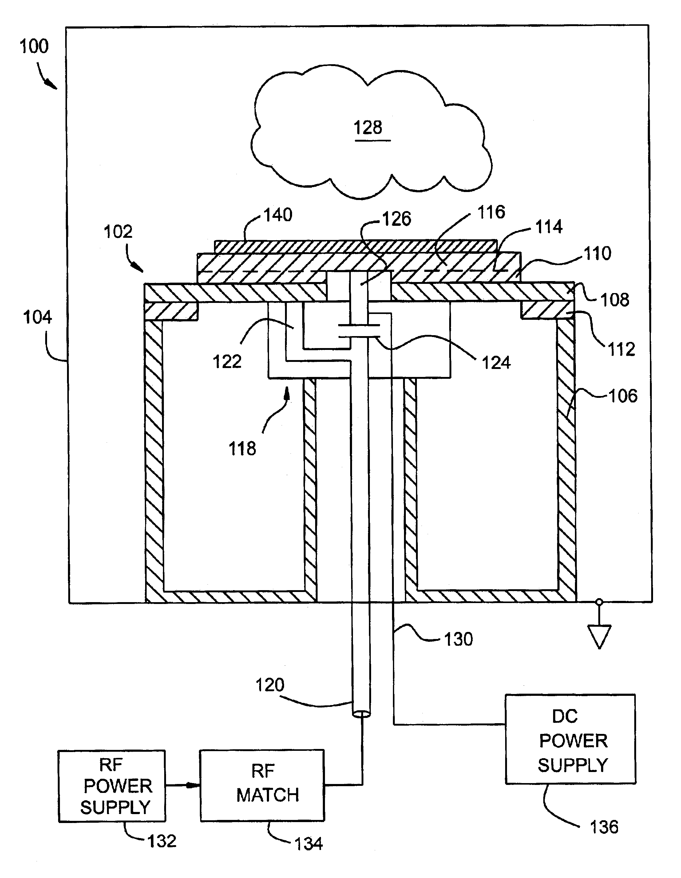
FIG. 1 depicts a schematic cross-sectional view of a prior art dual feed, cathode pedestal 102 of a plasma enhanced, semiconductor wafer processing chamber 100. The cathode pedestal 102 is positioned to support a semiconductor wafer or workpiece 140 within a vacuum vessel 104. The cathode pedestal 102 comprises a housing 106, a cooling plate 108, an insulator ring 112 and an electrostatic chuck 110. The electrostatic chuck 110 comprises an electrode 114 generally formed of molybdenum mesh embedded in a ceramic body 116. The electrostatic chuck 110 is mounted to the cooling plate 108 which rests on the insulator ring 112 above the housing 106. An RF feed structure 118 is coupled through the center of the housing 106 to the chuck electrode 114. The RF feed structure 118 comprises a first conductor 120, a second conductor 122, a capacitor bank 124, and a third conductor 126.

The first conductor 120, the capacitor bank 124 and the third conductor 126 are connected in series to couple RF ...


PUM

PropertyMeasurementUnit
frequencyaaaaaaaaaa
frequencyaaaaaaaaaa
drive frequencyaaaaaaaaaa

Abstract

A method and apparatus for routing harmonic energy within a plasma to ground in a plasma enhanced semiconductor wafer processing reactor. A model of the chamber is used to determine the pathway for RF power and the harmonic energy of that RF power through the chamber. From this model, the placement and design of a harmonic routing circuit is determined to shunt the harmonic energy to ground.

Description

BACKGROUND OF THE INVENTION1. Field of the InventionThe present invention generally relates to plasma enhanced semiconductor wafer processing chambers. More specifically, the invention relates to the method and apparatus for routing harmonics in a plasma to ground within a plasma enhanced semiconductor wafer processing chamber.2. Description of the Related ArtA plasma enhanced semiconductor wafer processing reactor generally comprises a vacuum vessel for containing one or more gases, a pedestal for supporting a semiconductor wafer or other workpiece within the vacuum vessel, and a power supply for applying energy to the gases to form a plasma within the vacuum vessel. Depending upon the structure of the vessel and the nature of the gases, processing within the vessel may include physical vapor deposition, chemical vapor deposition, plasma annealing or etching. In some chambers, particularly, a reactive ion etch chamber, the radio frequency (RF) power may be applied to the pedestal t...

Claims


Application Information

Patent Timeline
Patent Type & Authority Patents(United States)
IPC IPC(8): H01J37/32
CPCH01J37/32174H01J37/32082H01J37/00H01L21/02
Inventor SHANNON, STEVEN C.HOFFMAN, DANIEL J.BARNES, MICHAELLABLANC, LEE
Owner APPLIED MATERIALS INC
Why Eureka
Try Eureka