Method and apparatus for monitoring integrated circuit fabrication

Active Publication Date: 2005-04-12
ASML NETHERLANDS BV
View PDF105 Cites 61 Cited by
  • Summary
  • Abstract
  • Description
  • Claims
  • Application Information

AI Technical Summary

Benefits of technology

In one aspect, the present invention is a device, system and technique to shrink or reduce one, some or all ME into an EIW having suitable circuitry, structures, materials, capabilities and/or intelligence to perform one or some or all of those functions currently performed by conventional ME. In this way, capital equipment of at least part of the industry's infrastructure is reduced, minimized, and/or effectively or practically eliminated.
The EIW of the present invention may provide one, some or all of the following advantages:In-situ, holistic system-level monitoring. In this regard, the EIWs may sense and/or memorize and/or communicate while the process is taking place, the process information collected is in-situ. Time-sequence recording. The process information may be collected at different time points during th

Problems solved by technology

Notably, certain MEs may cause or requi

Method used


Image

  • Method and apparatus for monitoring integrated circuit fabrication
  • Method and apparatus for monitoring integrated circuit fabrication
  • Method and apparatus for monitoring integrated circuit fabrication

Examples


Embodiment Construction

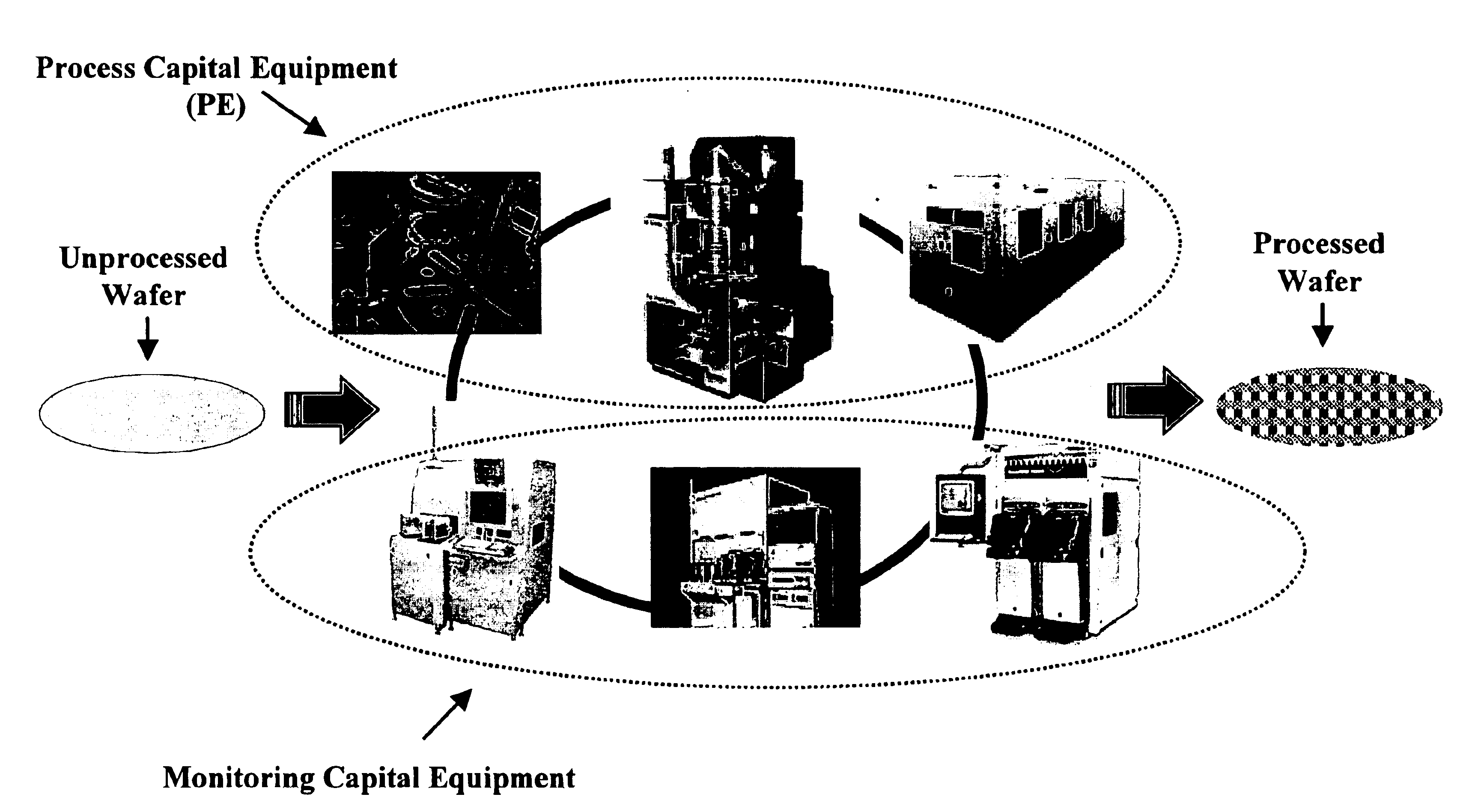
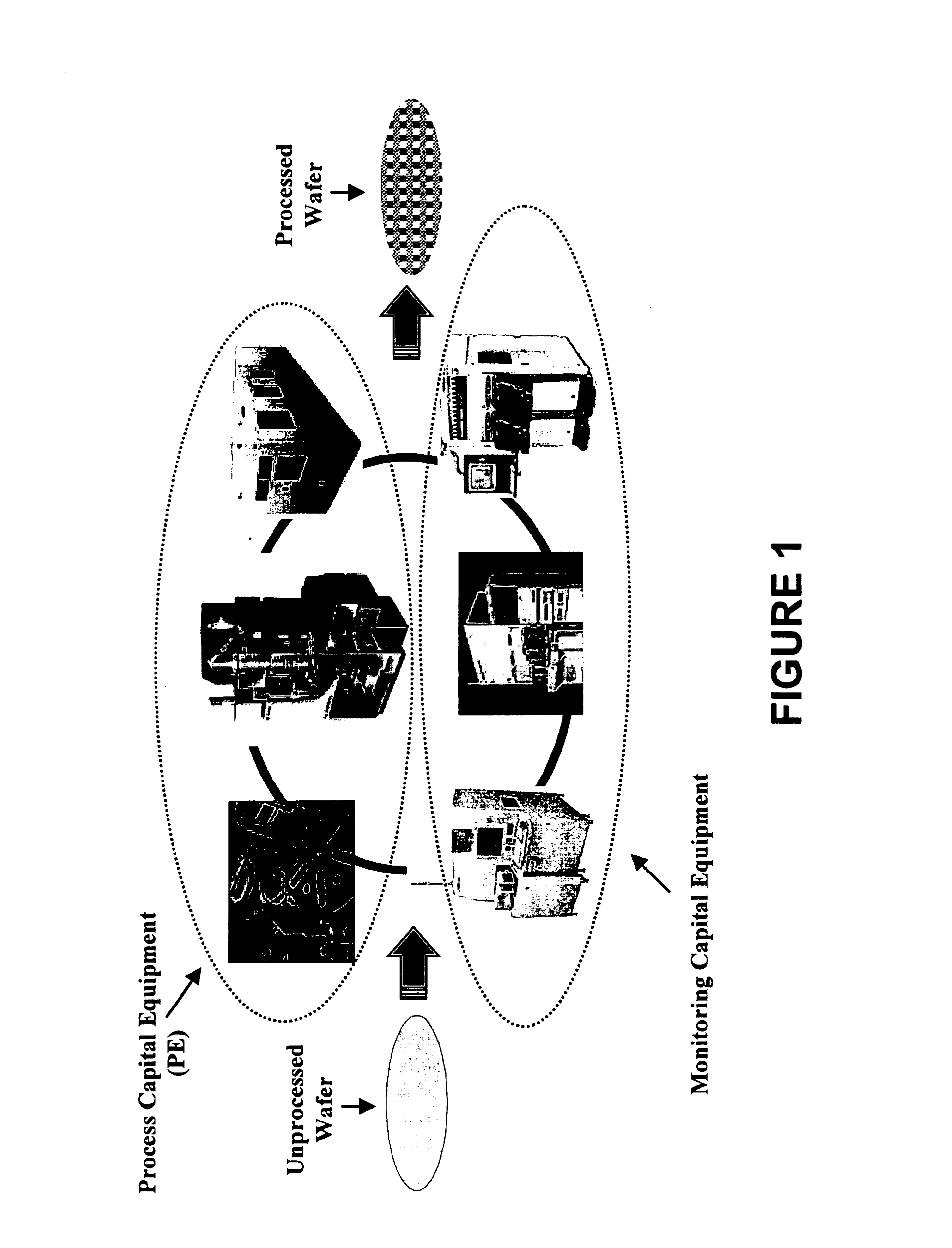
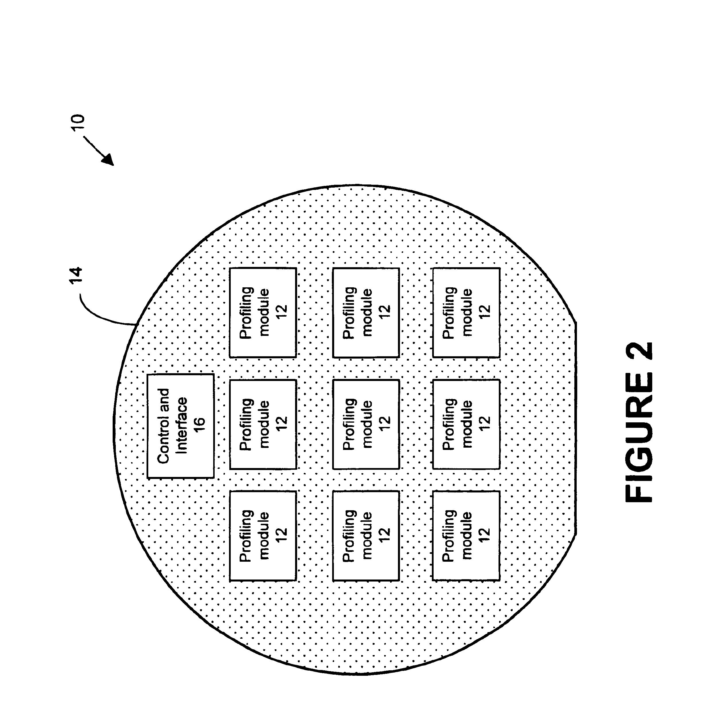
In one aspect, the present invention(s) is an Equipment-In-Wafer (“EIW”) having predetermined sources and / or sensors disposed and / or integrated on or in a wafer, a wafer-like substrate or a platform to sample, sense, detect, characterize, analyze and / or inspect certain parameters during a particular process(es) in the same or substantially the same environment as a product wafer (i.e., a wafer having actual integrated circuits fabricated thereon) would otherwise experience in processing or fabrication equipment, for example, integrated circuit processing or fabrication equipment.

In one embodiment, the EIW is a wafer or wafer-like object. When the EIW is a wafer-like object, the EIW may have a different physical form factor than a product wafer. The processing equipment, however, may handle such an EIW without adverse modification to its hardware and / or software. For example, where an EIW includes circuitry, sensors and / or sources to monitor a CVD process, the EIW may have the same o...


PUM

PropertyMeasurementUnit
Timeaaaaaaaaaa
Thicknessaaaaaaaaaa
Dielectric polarization enthalpyaaaaaaaaaa

Abstract

In one aspect, the present invention is a sensor unit for sensing process parameters of a process to manufacture an integrated circuit using integrated circuit processing equipment. In one embodiment, the sensor unit includes a substrate having a wafer-shaped profile and a first sensor, disposed on or in the substrate, to sample a first process parameter. The sensor unit of this embodiment also includes a second sensor, disposed on or in the substrate, to sample a second process parameter wherein the second process parameter is different from the first process parameter. In one embodiment, the sensor unit includes a first source, disposed on or in the substrate, wherein first source generates an interrogation signal and wherein the first sensor uses the interrogation signal from the first source to sample the first process parameter. The sensor unit may also include a second source, disposed on or in the substrate, wherein second source generates an interrogation signal and wherein the second sensor uses the interrogation signal from the second source to sample the second process parameter. The first sensor and the first source may operate in an end-point mode or in a real-time mode. In this regard, the first sensor samples the first parameter periodically or continuously while the sensor unit is disposed in the integrated circuit processing equipment and undergoing processing. In one embodiment, the first sensor is a temperature sensor and the second sensor is a pressure sensor, a chemical sensor, a surface tension sensor or a surface stress sensor.

Description

BACKGROUNDIntegrated circuit fabrication generally consists of a series of process steps or stages, for example, photolithography, etch, strip, diffusion, ion implantation, deposition, and chemical mechanical planarization (also known as chemical mechanical polishing, or “CMP”). At each step or stage, inspections and measurements are conducted to monitor the equipment which performs the process as well as the overall process, individual processes, and interaction and integration among individual processes.Typically supporting the integrated circuit fabrication process is a complex infrastructure of, for example, materials supply, waste treatment, support, logistics and automation. Integrated circuit fabrication processes tend to utilize one of the cleanest environments in the world.Integrated circuits are typically made on or in a semiconductor substrate that is commonly known as a wafer. A wafer is a substantially round, thin disk, having diameters such as four inches to twelve inc...

Claims


Application Information

Patent Timeline
IPC IPC(8): G01D9/00H01L21/00H01L23/544
CPCG01D9/005H01L21/67253H01L21/67276H01L22/34H01L2924/3011H01L2924/13091H01L2224/48463H01L2224/49107H01L2924/00
Inventor YE, JUNCHEN, XUN
Owner ASML NETHERLANDS BV
Why Eureka
Try Eureka