Semiconductor device producing method and semiconductor device

a semiconductor and micro-scale technology, applied in semiconductor devices, capacitors, electrical equipment, etc., can solve the problems of low etching rate of conductive films, ferroelectric memory cells cannot have a sufficient capacitor area, and cannot achieve high packing densities or integration, etc., to achieve the effect of increasing packing densities

Inactive Publication Date: 2005-04-19
SHARP KK
View PDF14 Cites 3 Cited by
  • Summary
  • Abstract
  • Description
  • Claims
  • Application Information

AI Technical Summary

Benefits of technology

[0010]Therefore, it is an object of the present invention to provide a semiconductor device having a micro-capacitor structure capable of addressing the increased packing densities and a method of producing a semiconductor device by which such a micro-capacitor structure is easily achieved.
[0019]In the method with the above process steps, a protuberant lower electrode having a sufficiently large height is achieved through the short-time etch-back of the insulation film by the CMP method and without using dry etching. In addition, because all of the upper and side surfaces of the thus achieved protuberant lower electrode are covered with the dielectric film and the upper electrode, the capacitor area is increased by the area of all the side surfaces of the lower electrode. Because the shape and size of the lower electrode is controlled by controlling the thickness of the insulation film and the shape and size of the hole, it is easy to obtain a narrow but high lower electrode. In addition, unlike the technique shown in FIG. 5, the dielectric film and the upper electrode are formed not inside of the lower electrode, but outside of it. Accordingly, it is possible to easily fabricate a very fine capacitor capable of accommodating to the increase in the packing densities, without reducing the capacitor area. Therefore, even though the hole formed in the insulation film is made very fine with reduction of the design rule, it is possible to form a three-dimensional capacitor having a sufficiently large capacitor area. Accordingly, it is possible to easily form a very fine capacitor coping with high integration and thus provide a ferroelectric memory cell enabling a DRAM level packing density.
[0030]In the method with the above process steps, a cud-shaped lower electrode having a sufficiently large height is achieved through the short-time etch-back of the first insulation film and the second insulation film (within the hole) by the CMP method and without using dry etching. In addition, because all of the inner and outer peripheries and the inner bottom surface of the thus achieved cup-shaped lower electrode are covered with the capacitor dielectric film and the upper electrode, a sufficiently large capacitor area is achieved. Because the shape and size of the lower electrode is controlled by controlling the thickness of the first insulation film and the shape and size of the hole, it is easy to obtain a narrow but high lower electrode.
[0031]The second conductive film may be formed such that a gap defined between opposite surfaces of the dielectric film within the hole is filled with a part of the second conductive film. Therefore, even though the hole formed in the first insulation film is made very fine with reduction of the design rule, it is possible to form a three-dimensional capacitor having a sufficiently large capacitor area. Accordingly, it is possible to easily form a very fine capacitor coping with high integration and thus provide a ferroelectric memory cell enabling a DRAM level packing density.
[0033]In either method of the present invention, if the barrier film is made of TiO2, Al2O3, or SiN, the barrier film well prevents a reaction between the dielectric film (capacitor dielectric film) and the interlayer insulating film.
[0036]Either method of the present invention may further comprise, after forming the insulation film (the first insulation film), forming a Ti film or a TiO2 film on the insulation film (the first insulation film). Such a film provides for good adhesion between the insulation film (the first insulation film) and the first conductive film. Thus, a semiconductor device produced can offer high reliability.

Problems solved by technology

However, the memory cell with this structure occupies a large area and is unsuitable for achieving high packing densities or integration.
Therefore, the ferroelectric memory cell is incapable of having a sufficient capacitor area if the memory cell has an area as small as less than a quarter micron.
Further, because its reaction product has a low volatility, the etching rate of the conductive film is low.
Thus the stacked capacitor structure has a problem that it is difficult to perform micro-processing.
The stacked capacitor structure has another problem that because the influence of a micro-loading effect is great in the case of a pattern of the order of less than submicron, the reaction product adheres to the conductive film and particles are developed on the conductive film.
Accordingly, it will be difficult to form the lower electrode, the ferroelectric film, and the upper electrode within the groove.

Method used


Image

  • Semiconductor device producing method and semiconductor device
  • Semiconductor device producing method and semiconductor device
  • Semiconductor device producing method and semiconductor device

Examples


first embodiment

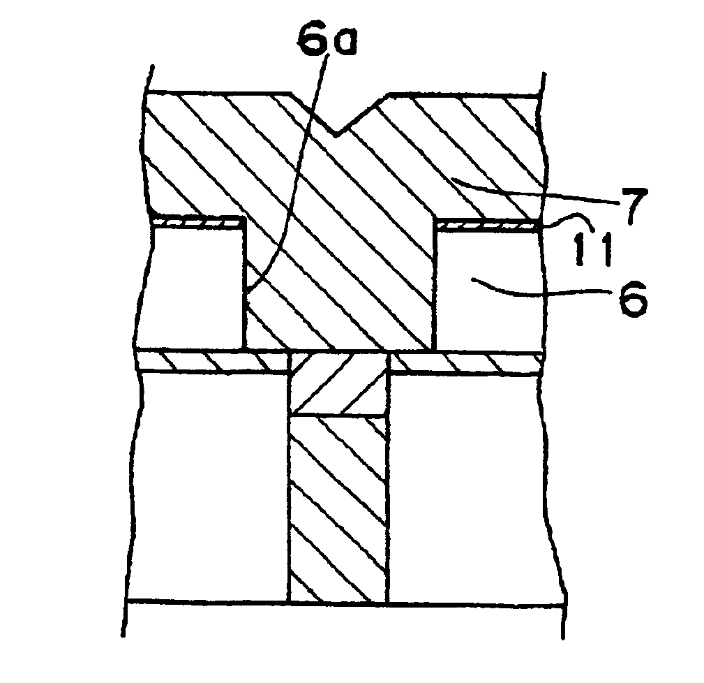
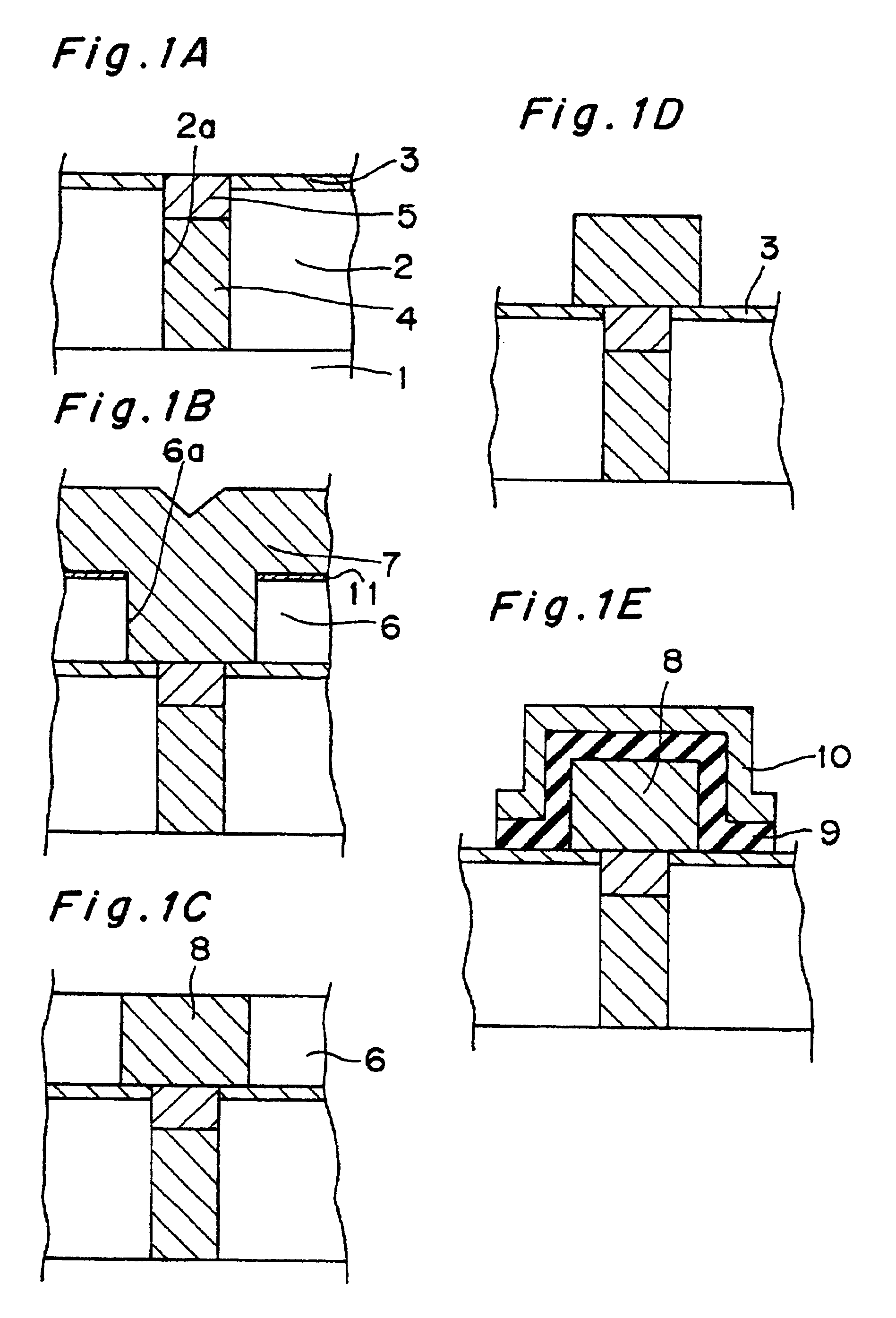
[0053]FIGS. 1A through 1E are sectional views of essential parts, showing steps of a semiconductor device production process according to a first embodiment of the present invention.

[0054]As shown in FIG. 1A, Si02 is deposited on a silicon substrate 1 on which transistors (not shown) have been formed, to form an interlayer insulating film 2 having a thickness of about 1-1.5 μm Thereafter, TiO2, Al2O3 or SiN is deposited on the interlayer insulating film 2 to form an underlying barrier film 3 having a thickness of about 0.05-0.2 μm. The underlying barrier film 3 fundamentally serves to prevent the reaction between a ferroelectric film and the SiO2 film 2.

[0055]Next, after a contact hole 2a is formed in the interlayer insulating film 2 and the underlying barrier film 3, doped polysilicon is deposited to the thickness of about 0.1-0.5 μm over the entire surface of the substrate. Thereafter, the doped silicon is etched by a RIE (reactive ion etching) method until the doped silicon on th...

second embodiment

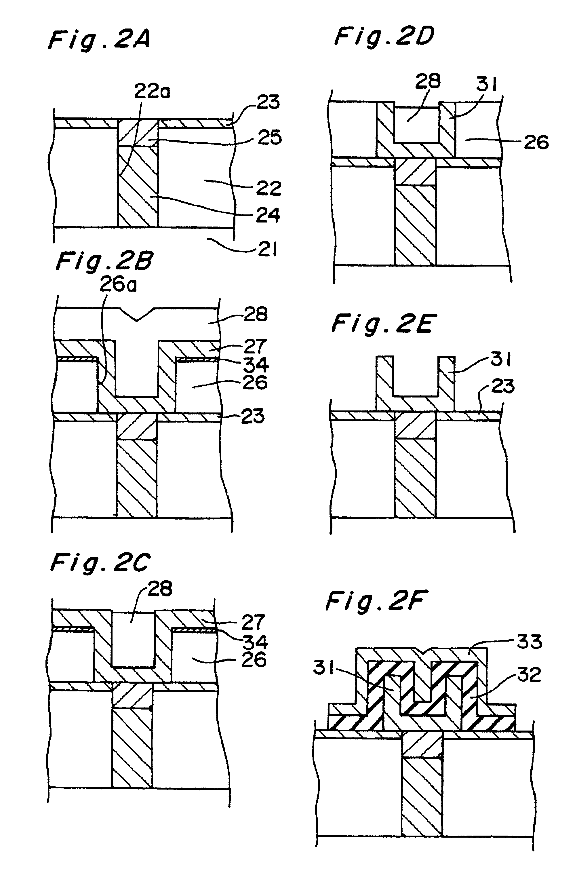
[0065]FIGS. 2A through 2F are sectional views of essential parts, showing steps of a semiconductor device production process according to a second embodiment of the present invention.

[0066]As shown in FIG. 2A, SiO2 is deposited on a silicon substrate 21 on which transistors (not shown) have been formed, to form an interlayer insulating film 22 having a thickness of about 1-1.5 μm. Thereafter, TiO2, Al2O3 or SiN is deposited on the interlayer insulating film 2 to form an underlying barrier film 23 having a thickness of about 0.05-0.2 μm. The underlying barrier film 23 fundamentally serves to prevent the reaction between a ferroelectric film and the SiO2 film 22.

[0067]Next, after a contact hole 22a is formed in the interlayer insulating film 22 and the underlying barrier film 23, doped polysilicon is deposited to the thickness of about 0.1-0.5 μm over the entire surface of the substrate. Thereafter, the doped silicon is etched by the RIE method until the doped silicon on the barrier f...


PUM


Abstract

In a semiconductor device producing method, a plug is formed within a contact hole formed in a barrier film and an interlayer insulating film on a semiconductor substrate. Then, an insulation film is formed on the plug and barrier film, and a hole is made in the insulation film such that an upper surface of the plug is exposed. A first conductive film is formed on the insulation film so as to fill the hole, and then etched by a CMP method to form a lower electrode within the hole. The insulation film is removed and the lower electrode is left in a protuberant manner. A dielectric film made of a ferroelectric or high-dielectric-constant substance and a second conductive film are sequentially formed over the lower electrode and the barrier film, and then patterned simultaneously to thereby form a capacitor dielectric film and an upper electrode.

Description

BACKGROUND OF THE INVENTION[0001]The present invention relates to a semiconductor device such as a ferroelectric memory cell, a DRAM, and the like and a method of producing the semiconductor device, and more particularly, to a method of forming a microscale capacitor for such a semiconductor device.[0002]As the semiconductor device, a ferroelectric memory cell having a one-transistor / one-capacitor structure is known. In the ferroelectric memory cell, a planar capacitor is formed over a transistor with an insulating film interposed therebetween. The transistor and the capacitor are completely isolated from each other. Therefore, after the capacitor is formed on the insulating film, the transistor and the capacitor are connected to each other locally with wiring. However, the memory cell with this structure occupies a large area and is unsuitable for achieving high packing densities or integration.[0003]To solve the problem, there has been proposed a ferroelectric memory cell having a...

Claims


Application Information

Patent Timeline
Patent Type & Authority Patents(United States)
IPC IPC(8): H01L21/02H01L27/10H01L21/8242H01L27/108
CPCH01L28/55H01L28/60H01L28/90H01L27/105
Inventor ONISHI, SHIGEO
Owner SHARP KK
Why Eureka
Try Eureka