Integrated circuit incorporating RF antenna switch and power amplifier

a technology of integrated circuits and power amplifiers, applied in the field of radio frequency (rf) communication systems, can solve the problems of poor isolation in the off state, unacceptably high performance cannot be achieved using external gaas based integrated circuits, etc., to reduce the insertion loss of switches, improve isolation, and eliminate most losses

Inactive Publication Date: 2005-04-19
TEXAS INSTR INC
View PDF12 Cites 115 Cited by
  • Summary
  • Abstract
  • Description
  • Claims
  • Application Information

AI Technical Summary

Benefits of technology

[0007]The present invention is a novel transmit / receive antenna switch capable of being integrated using silicon based RF CMOS semiconductor processes. The switch circuit is constructed whereby the substrate (i.e. bulk) terminals of the FETs are left floating, thus improving the isolation and reducing the insertion loss of the switch. The switch is combined with a power amplifier and both functions integrated within the same integrated circuit.
[0008]Floating the substrate of the transistors eliminates most of the losses caused by leakage paths through parasitic capacitances internal to the transistor, thus improving the isolation and reducing the insertion loss of the switch. Alternatively, the substrate is connected to the source or to ground via a resistor of sufficiently high value to effectively float the substrate, i.e. the resistance is sufficiently high to achieve similar switch performance as when the substrate is left completely floating.
[0009]The switch constructed using FETs with floating substrates enables the integration of RF transmit / receive antenna switches in the same CMOS RFICs containing the power amplifier. This integration of functions is very useful and even crucial to cost sensitive applications such as Bluetooth, WLANs and cordless telephones. This is achieved by the reduction in the cost of the transceiver through the elimination of the need for high cost external GaAs RFICs. Moreover, the integration of the antenna switch with the power amplifier in CMOS enables a reduction in size of the transceiver circuit that is important in small size portable wireless devices.
[0010]Note that in many cases, one skilled in the wireless communication circuitry arts can easily modify existing antenna switch and power amplifier designs to incorporate the present invention in order to achieve increased performance and / or cost reduction.

Problems solved by technology

Prior art attempts to integrate the transmit / receive antenna switch in a silicon CMOS process have resulted in switches having unacceptably high insertion losses when in the ON state and poor isolation in the OFF state.
Currently, such performance can only be achieved using external GaAs based RF integrated circuits.
Such integrated circuits are based on much more exotic semiconductor processes and are significantly more expensive than conventional silicon based semiconductor processes.
The low isolation characteristic of conventional silicon based integrated antenna switches, causes high leakage levels in the switch.
In a bi-directional switch this translates to the receive signal leaking into the transmit circuit from the antenna in addition to the leakage of the transmit signal into the receive circuit.

Method used


Image

  • Integrated circuit incorporating RF antenna switch and power amplifier
  • Integrated circuit incorporating RF antenna switch and power amplifier
  • Integrated circuit incorporating RF antenna switch and power amplifier

Examples


Embodiment Construction

Notation Used Throughout

[0020]The following notation is used throughout this document.

[0021]

TermDefinitionCMOSComplementary Metal Oxide SemiconductorDCDirect CurrentFETField Effect TransistorICIntegrated CircuitISMIndustrial Scientific Medical frequency bandPAPower AmplifierRFRadio FrequencyRFICRadio Frequency Integrated CircuitTDDTime Division DuplexingWLANWireless Local Area Network

DETAILED DESCRIPTION OF THE INVENTION

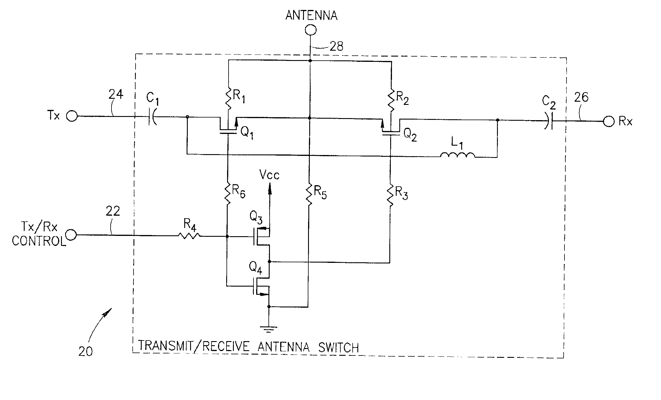
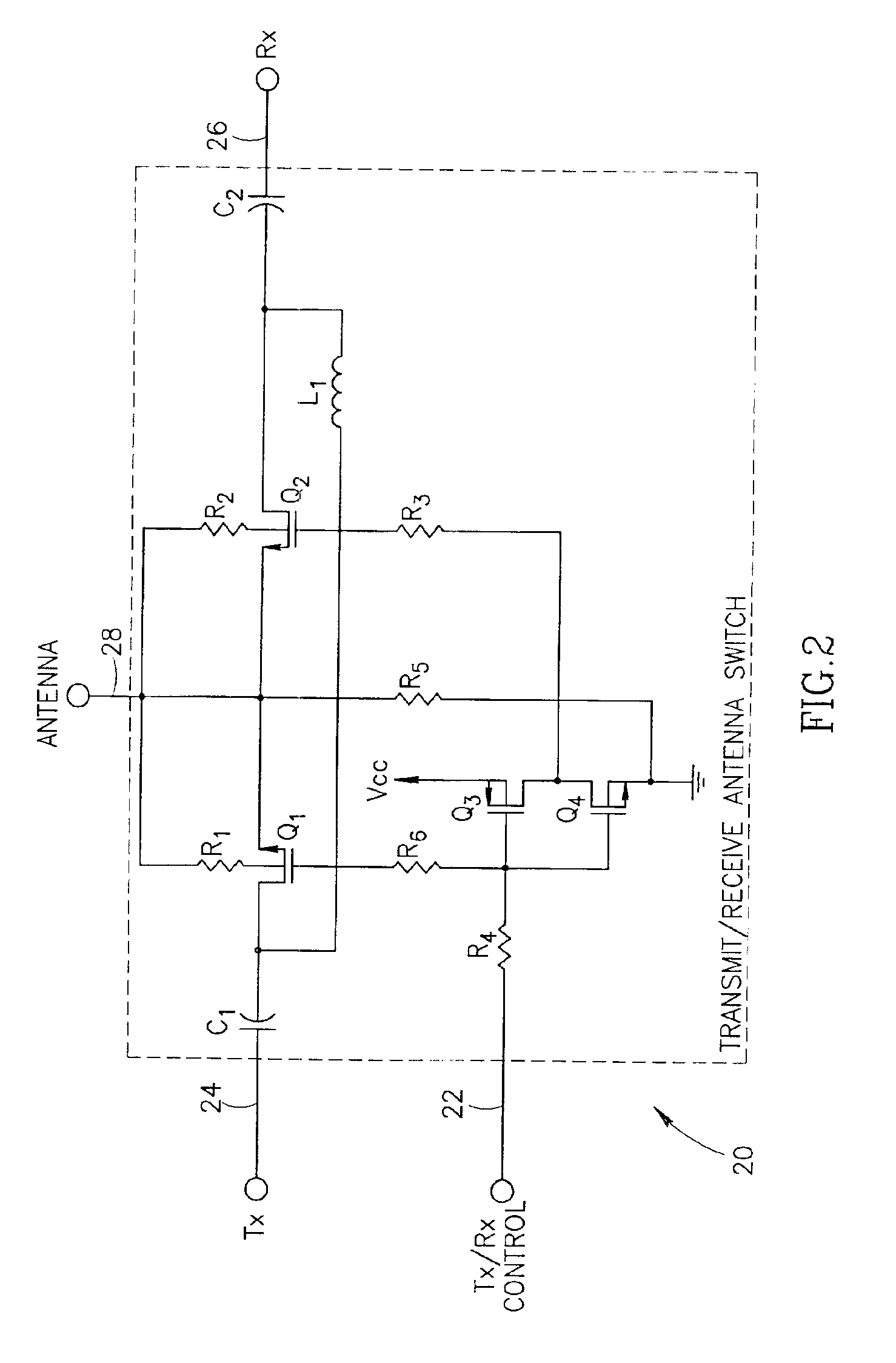
[0022]The present invention is a transmit / receive antenna switch capable of being integrated using silicon based RF CMOS semiconductor processes whereby the substrate (i.e. bulk) terminals of the FETs are left floating thus improving the isolation and reducing the insertion loss of the switch.

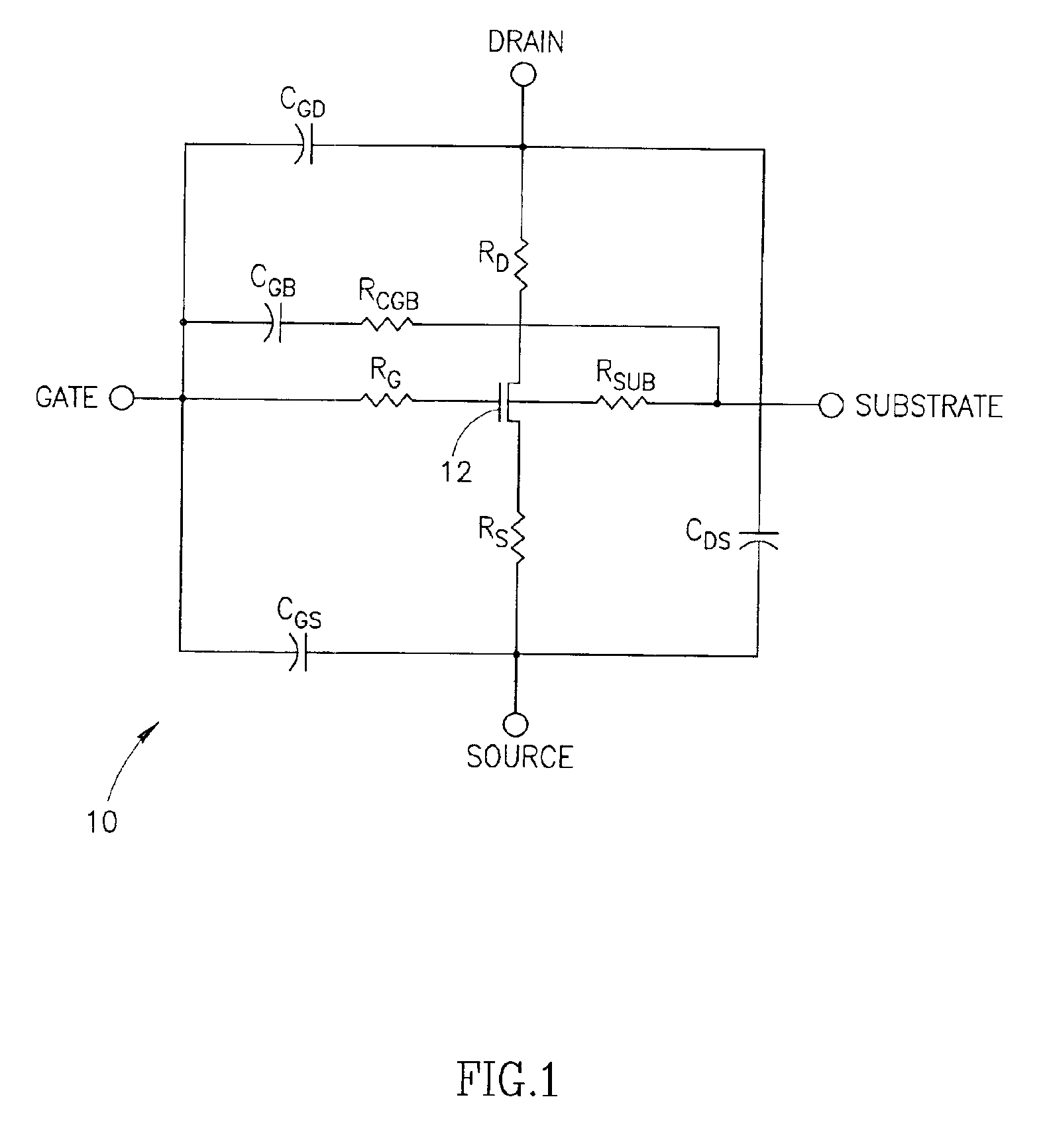
[0023]A schematic diagram of a circuit used to model a field effect transistor utilizing ideal components is shown in FIG. 1. The model of the FET, generally referenced 10, comprises an ideal field effect transistor 12 having a gate, source, drain and substrate terminals with re...


PUM


Abstract

A novel integrated circuit incorporating a transmit / receive antenna switch capable of being integrated using silicon based RF CMOS semiconductor processes and a power amplifier on the same substrate. The switch circuit is constructed whereby the substrate (i.e. bulk) terminals of the FETs are left floating thus improving the isolation and reducing the insertion loss of the switch. Floating the substrate of the transistors eliminates most of the losses caused by leakage paths through parasitic capacitances internal to the transistor thus improving the isolation and reducing the insertion loss of the switch. Alternatively, the substrate can be connected to the source or to ground via a resistor of sufficiently high value to effectively float the substrate.

Description

FIELD OF THE INVENTION[0001]The present invention relates generally to Radio Frequency (RF) communications systems and more particularly relates to an RF antenna switch constructed utilizing Field Effect Transistors (FETs) configured with floating substrate terminals wherein the switch and associated power amplifier are constructed in the same integrated circuit.BACKGROUND OF THE INVENTION[0002]Currently, high frequency radio frequency (RF) communications are becoming increasingly prevalent. Products touting wireless RF communication links are becoming increasingly popular among consumers. Today, there are an increasing number of new products, in addition to existing products being revamped that are being designed to incorporate wireless RF links.[0003]Due to the explosive consumer demand for products sporting wireless communication links, there is a need for low cost transceivers that are suitable for mass manufacture. In most wireless applications, especially those designed to be ...

Claims


Application Information

Patent Timeline
Patent Type & Authority Patents(United States)
IPC IPC(8): H04B1/44H04B1/48H04B1/04
CPCH04B1/48H04B1/04
Inventor MOSTOV, ALEXANDERLEIPOLD, DIRK
Owner TEXAS INSTR INC
Why Eureka
Try Eureka