Method of manufacturing device, device, and electronic apparatus

a manufacturing device and electronic equipment technology, applied in the direction of semiconductor devices, electrical equipment, transistors, etc., can solve the problems of low raw material utilization efficiency, low productivity, and difficult handling

Inactive Publication Date: 2005-04-26
SEIKO EPSON CORP
View PDF5 Cites 63 Cited by
  • Summary
  • Abstract
  • Description
  • Claims
  • Application Information

AI Technical Summary

Benefits of technology

[0024]Further, the present invention provides the method of manufacturing a device, wherein the step of heating at a high tempera

Problems solved by technology

However, the CVD method has problems in that a large-scaled apparatus is required, the utilization efficiency of raw materials is low, the handling is difficult due to the use of gaseous raw materials, and a large quantity of waste is produced.
Also, the sputtering method has problems common to the CVD method in that the film thickness at an uneven portion on a surface of a substrate is non-uniform, the productivity is low, and an apparatus is large-scale and expensive due to the required vacuum apparatus.
However, this method has the following problems.
That is, since vaporizing and cooling silicon hydride as a raw material is carried out continuously, a complicated apparatus is not only required but also the control of film thickness is difficult.
However, in this method, since materials having a low molecular weight are used, the system is unstable and thus the handling thereof is difficult.
Furthermore, since the solution used in this method has a bad wettability to the substrate, the application thereof to the substrate is inherently difficult.
In addition, since the materials have a low molecular weight, the boiling point thereof is low and thus the

Method used


Image

  • Method of manufacturing device, device, and electronic apparatus
  • Method of manufacturing device, device, and electronic apparatus
  • Method of manufacturing device, device, and electronic apparatus

Examples


embodiments

[0113]Now, although the present invention will be described in detail in conjunction with embodiments, the present invention is not limited to such embodiments.

first embodiment

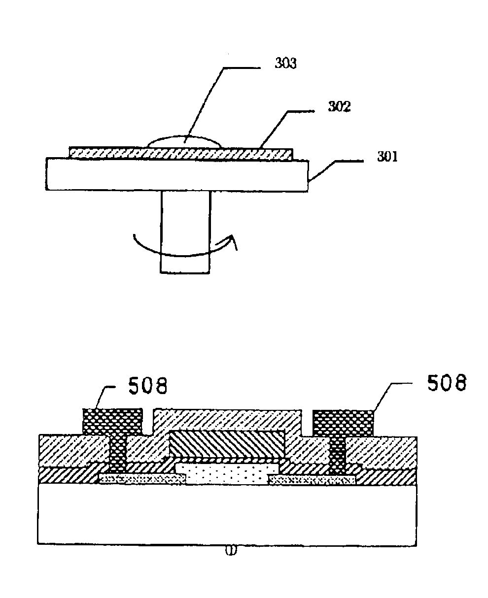
[0114]A first embodiment of the present invention is shown in FIG. 4. FIG. 4 illustrates a process of manufacturing a coplanar type thin film transistor according to the first embodiment of the present invention. In FIG. 4(a), on a glass substrate 401 on which an insulating film 412 is previously formed as a base, an applied film is formed at the rate of revolution of 500 rpm using as a liquid material a solution refined by filtering with a 1 μm filter the liquid material (high-order silane solution) after irradiating with TV rays of 20 mW / cm2 having a wavelength of 308 nm for 20 minutes to a benzene solution of 50 ml containing 15 wt % of cyclopentasilane. Next, after carrying out a heat treatment at 100° C. for 20 minutes to remove the solvent of the applied film, a heat treatment is carried out again at 400° C. for 30 minutes to make the applied film into a metallic silicon film. Next, the laser annealing with an energy density of 300 mJ / cm2 is carried out to form a polycrystalli...

second embodiment

[0124]A second embodiment of the present invention is shown in FIG. 5. FIG. 5 illustrates a process of manufacturing a staggered type thin film transistor according to the present invention. In FIG. 5(a), reference numeral 501 indicates a glass substrate and reference numerals 502 and 503 indicate doped silicon films which will become the source / drain regions and which dopants are doped in. The formation of the doped silicon films is carried out as follows. That is, as liquid material (high-order silane solution) obtained by irradiating with UV rays of 15 mW / cm2 having a wavelength of 436 nm for 15 minutes a toluene solution of 50 ml containing 30 wt % of cyclopentasilane, adding decaborane of 0.5 g to the solution and then filtering the resultant solution with a 0.5 μm filter, is applied to form an applied film. Subsequently after carrying out an heat treatment at 150° C. for 30 minutes to remove the solvent of the applied film, a heat treatment is carried out again at 350° C. for ...


PUM


Abstract

A method of manufacturing a device comprising individual thin films including a silicon film, a gate insulating film, a conductive film for a gate electrode, an interlayer insulating film, and a conductive film for an electrode and wiring, comprising: a step of applying a liquid material to form an applied film; and a heat treatment and/or a light irradiating treatment of making the applied film into the silicon film, wherein, as the liquid material, a high-order silane composition comprising a high-order silence formed by photopolymerization by irradiating a silane compound solution having a photopolymerization property with UV rays is used.

Description

BACKGROUND OF THE INVENTION[0001]1. Technical Field of the Invention[0002]The present invention relates to a method of manufacturing a device which is employed in electronic apparatuses, such as a liquid crystal display device (for example, a small-sized LCD or a large-sized LCD), a self light-emitting display device (for example, an organic EL display or a plasma display), and an LSI, and more specifically, to a method of manufacturing a device by forming thin films constituting the device using liquid materials, to a device obtainable through the method, and to an electronic apparatus comprising the device.[0003]2. Description of the Related Art and Problems to be Solved by the Invention[0004]In general, devices such as a thin film transistor comprise thin films, such as a semiconductor film, an insulating film or a conductive film. In a liquid crystal display device or the like, a transparent conductive film is also employed except the above films. Classifying these thin films in...

Claims


Application Information

Patent Timeline
IPC IPC(8): H01L21/02H01L29/66H01L21/336H01L21/3205H01L21/208H01L29/786H01L21/20H01L21/288
CPCH01L21/32055H01L29/66757H01L29/78618H01L21/02628H01L21/02636H01L21/02532H01L27/1292
Inventor AOKI, TAKASHIFURUSAWA, MASAHIROYUDASAKA, ICHIO
Owner SEIKO EPSON CORP
Why Eureka
Try Eureka