Circuit isolation utilizing MeV implantation

a technology of circuit isolation and implantation, applied in the direction of semiconductor devices, semiconductor/solid-state device details, electrical apparatus, etc., can solve the problems of increased cross-talk problems, increased cost due to separate packaging and increased pin counts, and increased steps compared to standard cmos processes. achieve the effect of reducing resistan

Inactive Publication Date: 2005-04-26
AVAGO TECH WIRELESS IP SINGAPORE PTE
View PDF33 Cites 19 Cited by
  • Summary
  • Abstract
  • Description
  • Claims
  • Application Information

AI Technical Summary

Benefits of technology

[0013]The present invention may further comprise a method of isolating circuits to be formed or a common substrate of a wafer comprising the steps of forming a mask in predetermined locations on the wafer that are aligned with isolated regions between the circuits, irradiating the wafer with ions having an energy level sufficient to implant the ions in embedded regions of the common substrate that are substantially aligned with unmasked portions of the wafer so that the isolated regions are formed between the circuits and the embedded regions are buried in the common substrate and have a lower resistance than the common substrate so that currents injected into the common substrate by a particular circuit preferentially flow to a ground potential of the particular circuit rather than through the isolation region that has a higher resistance.
[0014]The present invention may further comprise an integrated circuit having a plurality of circuits formed on a common substrate that are isolated by isolation regions in the common substrate between the circuits, the integrated circuit made by the process of masking predetermined locations of the common substrate that are substantially aligned with the isolation regions with a material that is capable of masking high energy ions, irradiating the common substrate with the high energy ions such that the high energy ions have an energy level sufficient to implant the high energy ions in embedded regions of the common substrate that are aligned with unmasked portions of the common substrate, said unmasked portions being aligned with the circuits so that the isolation regions are formed between the embedded regions and the embedded regions are buried in the common substrate so that a portion of the common substrate separates the embedded regions from the circuits.
[0015]The present invention may further comprise an integrated circuit comprising a common substrate having low doping and a first predetermined resistance, circuitry formed on predetermined portions of the common substrate, embedded regions of the common substrate that are implanted with ions such that the embedded regions have a resistance that is lower than the first predetermined resistance, the embedded regions being substantially aligned with the circuitry and buried in the common substrate so that a portion of the common substrate separates the embedded regions from the circuitry.
[0016]The present invention may further comprise a silicon wafer suitable for the formation of integrated circuits comprising a common substrate on which the integrated circuits can be formed in predetermined locations on the common substrate, the common substrate having a first predetermined resistance, embedded regions of implanted ions deposited in the common substrate that are substantially aligned with the predetermined locations on the common substrate, the embedded regions having a resistance that is lower than the first predetermined resistance and buried in the common substrate so that a portion of the common substrate separates the embedded regions from the predetermined locations on which the circuits can be formed.

Problems solved by technology

When epitaxial wafers are used, the substrate normally has a lower resistance so that cross-talk problems are increased.
This adds cost due to separate packaging and increased pin counts.
However, these steps are costly compared to standard CMOS processes.
Other alternatives rely on circuit design techniques, such as current-mode logic, or spacing of the unrelated circuits, but circuit noise isolation is still difficult to achieve using these alternatives.

Method used


Image

  • Circuit isolation utilizing MeV implantation
  • Circuit isolation utilizing MeV implantation
  • Circuit isolation utilizing MeV implantation

Examples


Embodiment Construction

[0029]While this invention can be implemented in various embodiments, the drawings illustrate, and the specification describes, detailed specific embodiments that are provided for the purpose of understanding that the present disclosure is to be considered as an exemplification of the principles of the invention, but is not to be limited to the specific embodiments described.

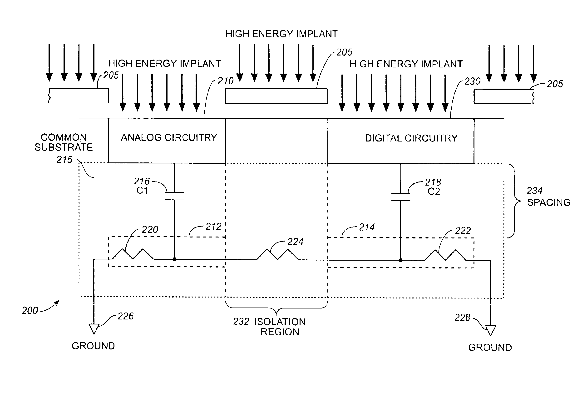
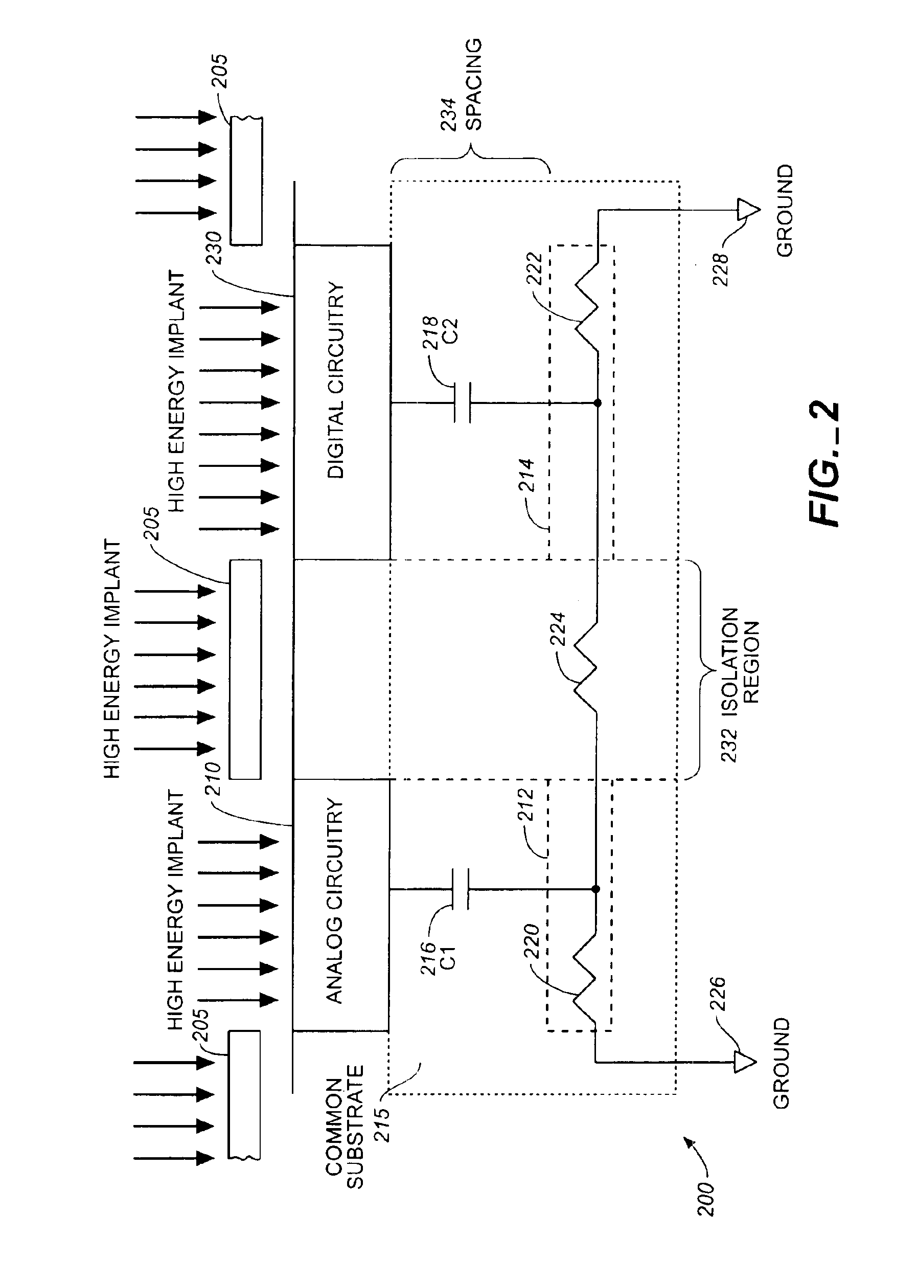
[0030]FIG. 2 illustrates an integrated circuit 200 according to the present invention. Substrate 215 is preferably part of a bulk substrate wafer with a high resistivity or may comprise an epitaxial layer having an underlying layer. Prior to the formation of any circuits, a high energy implant mask 205 is disposed on the surface of substrate 215 so that unmasked portions are substantially aligned with the circuits 210, 230, as illustrated. High energy implant mask 205 may comprise a silicon dioxide film, silicon nitride film or, as disclosed in more detail in FIG. 10, a combination of a hard masking material and...


PUM


Abstract

A circuit isolation technique that uses implanted ions in embedded portions of a wafer substrate to lower the resistance of the substrate under circuits formed on the wafer or portions of circuits formed on the wafer to prevent the flow of injected currents across the substrate. The embedded ions provide low resistance regions that allow injected currents from a circuit to flow directly to a ground potential in the same circuit rather than flowing across the substrate to other circuits. High energy implantation processes on the order of 1 MeV to 3 MeVs can be used to implant the ions in embedded regions. Multiple energy levels can be used to provide thick embedded layers either prior to or after application of an epitaxial layer. Various masking materials can be used to mask the isolation regions during the implantation process, including hard masking materials such as silicon dioxide or silicon nitride, poly-silicon or an amorphous silicon layer, and a photoresist layer. Additive materials can be used in one or more of the masking layers to increase the absorption characteristics of the high energy ions. Separate physical masks can be used to block the implantation of ions.

Description

CROSS-REFERENCE TO RELATED APPLICATIONS[0001]This application is based upon and claims priority of U.S. nonprovisional application Ser. No. 09 / 264,286, entitled “CIRCUIT ISOLATION UTILIZING MeV IMPLANTATION”, filed Mar. 8, 1999 by Donald M. Bartlett, Gayle Miller and Rudy Mason, the entire disclosure of which is herein specifically incorporated by reference for all that it discloses and teaches.FIELD OF THE INVENTION[0002]The present invention relates to isolating circuits and more particularly to noise isolating between unrelated circuits on an integrated circuit.BACKGROUND OF THE INVENTION[0003]Noise isolation between unrelated circuits on an integrated circuit (IC) is highly desirable. This is particularly true when high power circuits and low power circuits are on the same IC. For example, low power circuits may process minimal signals (<10 mV) and cannot tolerate interference generated by high power circuits on the same IC. FIG. 1 illustrates one of the mechanisms in which c...

Claims


Application Information

Patent Timeline
Patent Type & Authority Patents(United States)
IPC IPC(8): H01L21/265H01L21/02H01L21/70H01L21/76H01L21/266H01L21/8238
CPCH01L21/26513H01L21/266H01L21/76H01L21/823878Y10S257/92Y10S438/942Y10S438/948
Inventor BARTLETT, DONALD M.MILLER, GAYLE W.MASON, RANDALL J.
Owner AVAGO TECH WIRELESS IP SINGAPORE PTE
Why Eureka
Try Eureka