

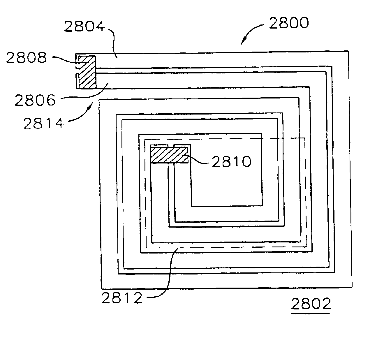
Multi-track integrated spiral inductor
a spiral inductor and multi-track technology, applied in the field of receiver circuits, can solve the problems of difficult to account for radio signals, difficult to design a receiver, and distortion of captured signals,
- Summary
- Abstract
- Description
- Claims
- Application Information
AI Technical Summary
Benefits of technology
Problems solved by technology
Method used
Image

Examples
Embodiment Construction
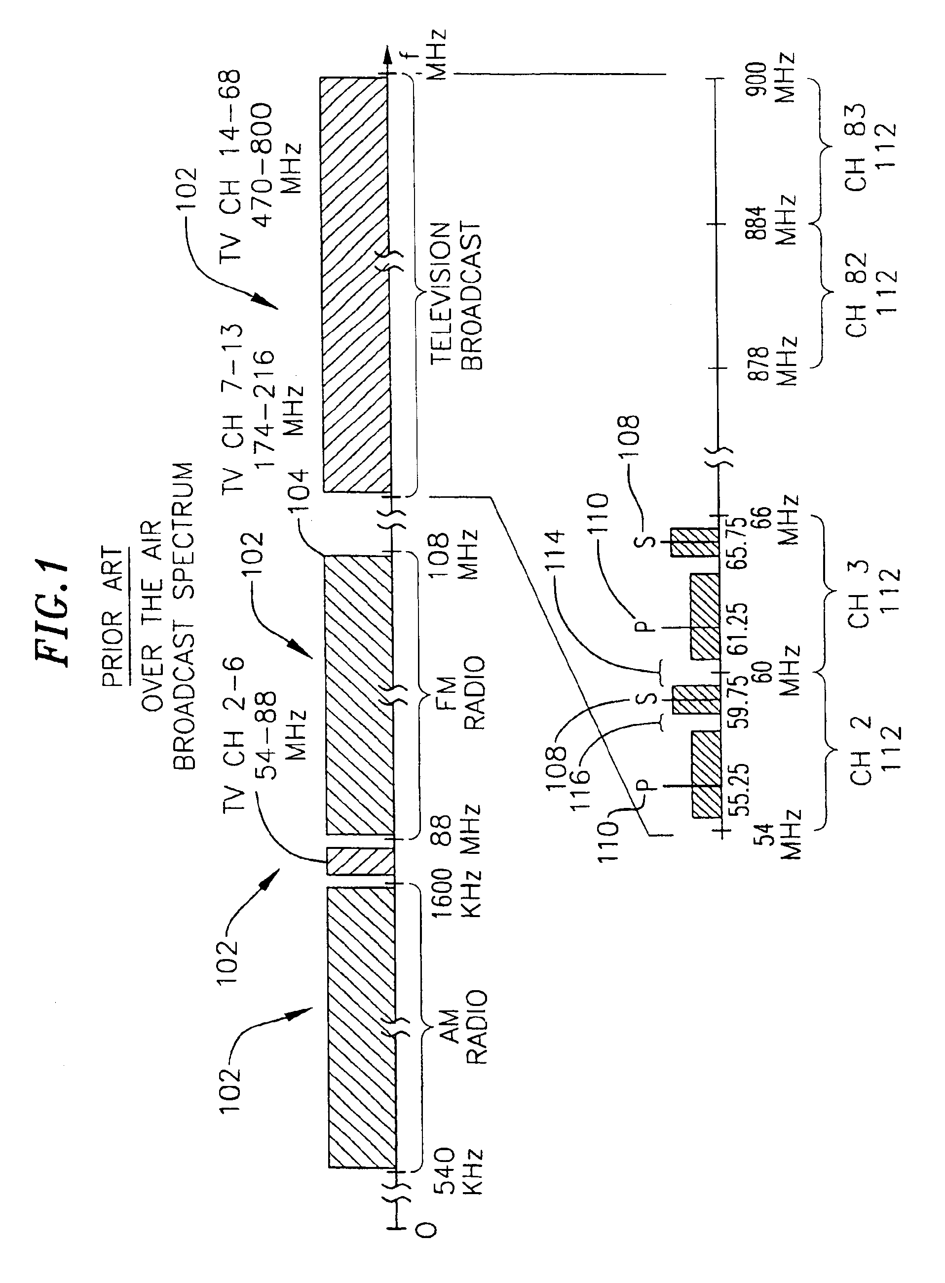
[0100]FIG. 1 is an illustration of a portion of the radio frequency spectrum allocations by the FCC. Transmission over a given media occurs at any one of a given range of frequencies that are suitable for transmission through a medium. A set of frequencies available for transmission over a medium are divided into frequency bands 102. Frequency bands are typically allocations of frequencies for certain types of transmission. For example FM radio broadcasts, FM being a type of modulation, is broadcast on the band of frequencies from 88 MHz to 108 MHz 104. Amplitude modulation (AM), another type of modulation, is allocated the frequency band of 540 kHz to 1,600 kHz 106. The frequency band for a type of transmission is typically subdivided into a number of channels. A channel 112 is a convenient way to refer to a range of frequencies allocated to a single broadcast station. A station broadcasting on a given channel may transmit one or more radio frequency (RF) signals within this band t...
PUM
| Property | Measurement | Unit |
|---|---|---|
| frequencies | aaaaa | aaaaa |
| frequencies | aaaaa | aaaaa |
| frequency | aaaaa | aaaaa |
Abstract
Description
Claims
Application Information