Contact element for use in electroplating

a contact element and electroplating technology, applied in the field of contact elements, can solve the problems of difficult practical solutions, large currents that cannot be transmitted onto the thin conductive base coating of the device is not suited for transmitting large electric currents to the printed circuit board, so as to improve the cooling effect, and reduce the effect of heat generation

Inactive Publication Date: 2005-05-03
ATOTECH DEUT GMBH
View PDF29 Cites 15 Cited by
  • Summary
  • Abstract
  • Description
  • Claims
  • Application Information

AI Technical Summary

Benefits of technology

[0034]The inventive embodiments of the contact element have the advantage desired. The reason why this is so is not known, though. But it has been assumed that the selected arrangement allows better cooling of the contact spots and a more uniform supply of large currents, to very thin layers of metal in particular. On account of the longer boundary line, the current density flowing at the transition between the contact spots and the work is lower. Normally, the current flowing through the contact spots on the surfaces of the printed circuit boards considerably heats the material. It is possible that it is this rise in temperature that occasions the damage or destruction caused to the printed board material. By having the inventive contact elements provided with several humps fitted with contact surfaces separated by intervals or by giving the contact areas regular or irregular geometrical shapes, the liquid for treatment is better capable of contributing to cool the contact spots than in the case with the contact elements of the prior art which have und

Problems solved by technology

This device is not suited for transmitting large electric currents to the printed circuit boards.
It is also difficult to find a solution for practical operation that, on one hand, provides the brushes with a long working life and that, on the other hand, protects the surfaces of the printed circuit boards against damage.
If, for the electrolytic treatment of printed circuit boards coated with copper on both sides, clamps that grasp both sides and supply electric contact are used, one such clamp carries 40 to 160 A. Such large currents are difficult to be transmitted onto the thin conductive base coating of the boards.
These increasing demands placed on the modern fabrication of printed circuits are no longer to be met with the devices of the art.
This mean

Method used


Image

  • Contact element for use in electroplating
  • Contact element for use in electroplating
  • Contact element for use in electroplating

Examples


first embodiment

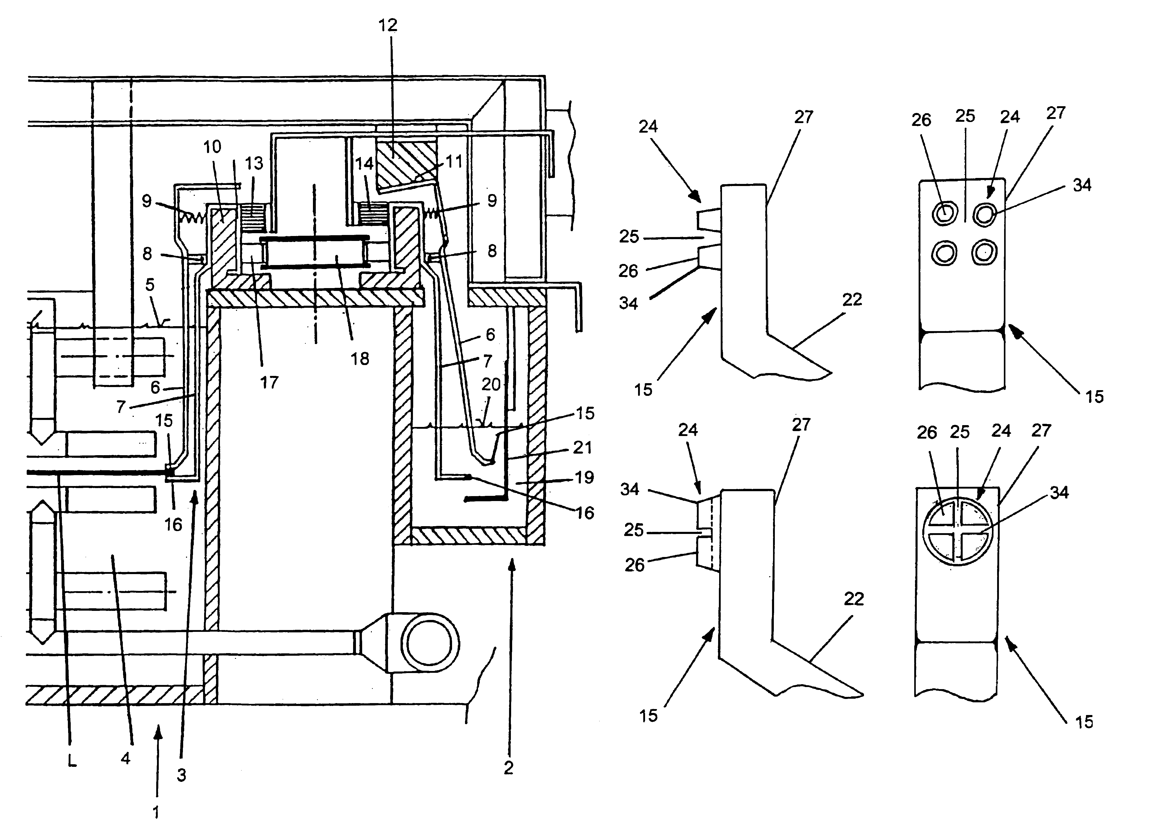
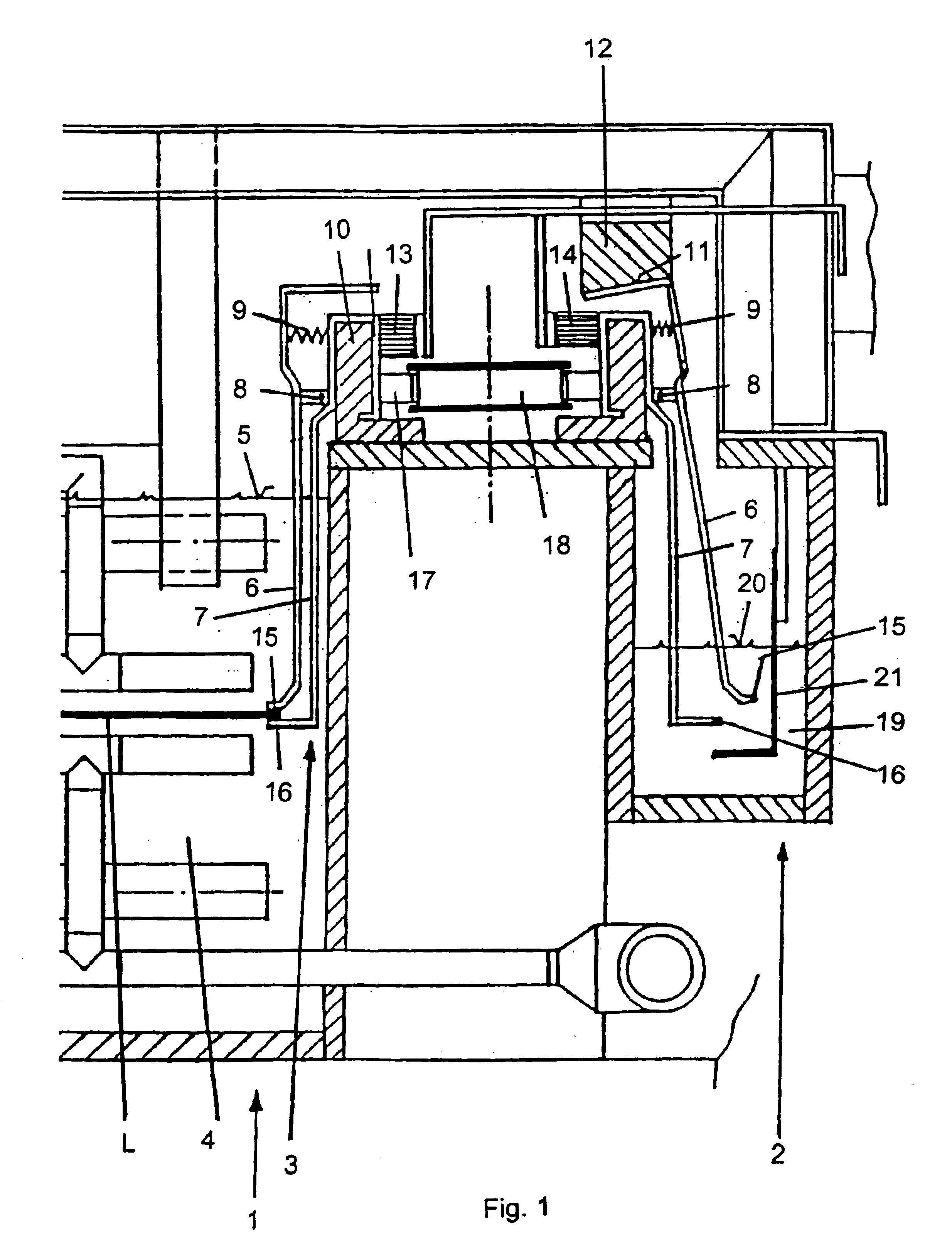
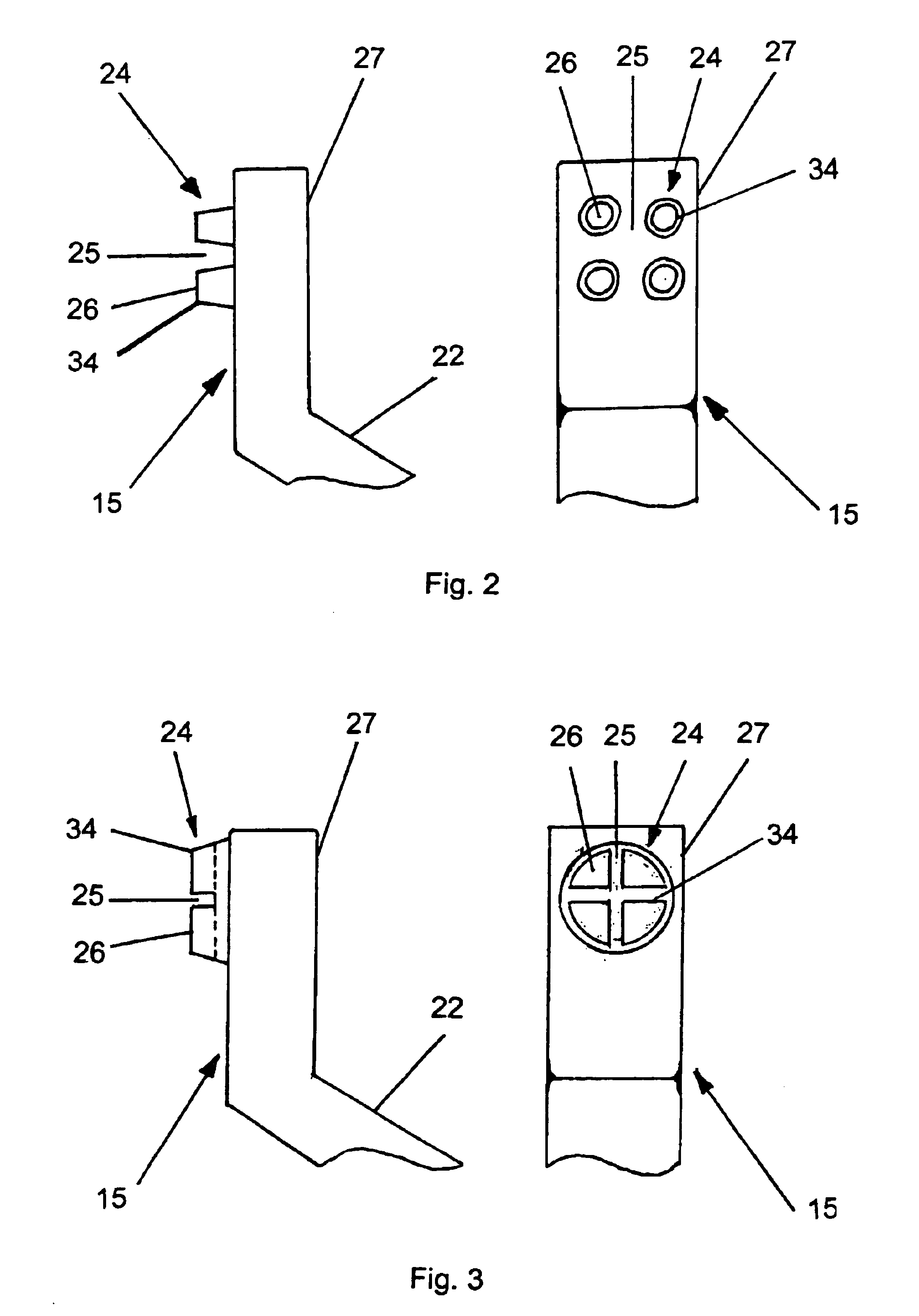
[0060]a contact element 15 according to the invention is shown in FIG. 2. The contact element 15 is fastened to the stem 22 of the external clamp bar 6. The contact element 16 (not here presented) is fastened to the stem 23 of the internal clamp bar 7 in like manner. The contact elements 15, 16 substantially consist of a contact foot 27 and of the humps 24 fastened there onto with intervals 25 provided in between. Four humps 24 are provided in this embodiment, said humps being arranged on the corners of a square. On one side the contact humps 24 are provided with contact areas 26 which are delimited by the boundary line 34. On closing the clamp 3, the contact areas 26 are printed, i.e. pressed, very strongly on corresponding contacting areas on the surfaces of the printed circuit boards. The planarity of the contact areas 26 permits to achieve an intimate electrical contact with very little contact resistance between the contact areas of the humps 24 and the surfaces of the printed ...

second embodiment

[0062]the contacts is illustrated in FIG. 3. In this case too, the contact elements 15 (16 not shown) consist of the contact foot 27 and of the humps 24 arranged on said contact foot 27. In this case, the humps 24 are produced out of a circular surface in which grooves 25 are cut, which form the intervals between the humps 24. In this case there are two right-angled grooves 25 which subdivide the originally circular surface into four symmetrically arranged humps 24, each having the shape of a segment of a circle. In this case as well the various humps 24 are provided on one side with contact areas 26 which are delimited by the boundary line 34.

third embodiment

[0063]FIG. 4 indicates a third embodiment for the contacts. In this case, the contact foot 27 of the contact elements 15 (16 not shown) has an elongate shape. The various humps 24 are arranged in a row-shaped matrix and are produced by cuttings that simultaneously form the intervals (grooves) 25. The humps 24 are again provided on one side with plane contact areas 26 which are delimited by the boundary line 34.

[0064]The elongate shape of the hump arrangement allows a large supporting surface to be formed on a very narrow galvanoedge, a large enough contact surface F being available at the same time. As a result, the width of the useless galvanoedge may be further reduced.

[0065]The embodiments of FIGS. 2-4 are illustrative of embodiments of the present invention wherein the shape of the contact areas 26 is designed in such a way that the ratio V of the square of the overall length L of all boundary lines 34 to the size F of all the contact areas 26 as given by the expression: V=L2F

is...


PUM

PropertyMeasurementUnit
Electrical conductivityaaaaaaaaaa
Electrical resistanceaaaaaaaaaa
Currentaaaaaaaaaa

Abstract

It is difficult to transmit large processing current on the surfaces of printed circuit boards (L) using clamp-type contact organs (6, 7). In order to solve said problem, contact elements (15, 16) having one or more contact surfaces (26) are disposed on the contact organs (6, 7). The shape of the contact surfaces (26) are configured in such a way that no damages occur in the areas of the conductive surfaces adjacent to the contact surfaces (26) when large currents are transmitted from the contact elements (15, 16) printed on the electrically conductive surface of printed board material (L) on the contact surfaces to the conductive surface.

Description

BACKGROUND OF THE INVENTION[0001]1. Field of the Invention[0002]The invention relates to a contact element for supplying electric current to substantially board-shaped objects that are to be treated by an electrolytic process.[0003]2. Brief Description of the Related Art[0004]To submit objects to an electrolytic treatment, they have to be transported and placed in electric contact in order for them to be supplied with electric current while being in contact with a liquid for treatment.[0005]Various appliances are used to serve this purpose. U.S. Pat. No. 4,767,146 for example discloses holding tongs for printed circuit boards which comprise two legs provided each with two gripping arms. On account of the force of a spring, the legs with the gripping arms are pivotal about an upper axis, the lower ends being thus pushed together. The lower ends of the gripping arms are provided with teeth. The arms of the one leg are provided with two tooth-like projections each and the arms of the o...

Claims


Application Information

Patent Timeline
IPC IPC(8): C25D17/06C25D5/00H05K3/24C25D17/00H05K3/18
CPCC25D17/06H05K3/241C25D17/005C25D17/001C25D17/004C25D7/123C25D17/00
Inventor LANGHEINRICH, PETER
Owner ATOTECH DEUT GMBH
Why Eureka
Try Eureka