Method of manufacturing flash memory

Active Publication Date: 2005-05-03
MACRONIX INT CO LTD
View PDF10 Cites 2 Cited by
  • Summary
  • Abstract
  • Description
  • Claims
  • Application Information

AI Technical Summary

Benefits of technology

[0013]Accordingly, one object of the present invention is to provide a method of fabricating a flash memory device that protects the inter-gate dielectric layer against any harmful damage so that average performance of the device is improved.
[0014]A second object of this invention is to provide a method of fabricating a flash memory device that prevents any polymer residue from contaminating nearby gate layers and thus improves the quality of the gate.
[0016]In the aforementioned method, a passivation layer is formed over the inter-gate dielectric layer above the memory cell region. The passivation layer is able to protect the inter-gate dielectric layer against any possible processing damage so that the quality of the inter-gate dielectric layer can be maintained.
[0017]Furthermore, by forming a passivation layer over the inter-gate dielectric layer, stronger chemical agents can be deployed to remove photoresist in a cleaning process. As a result, there will be very little polymer residue to contaminate surrounding gate layers after the cleaning step.

Problems solved by technology

In the aforementioned fabrication process, the inter-gate dielectric layer 112 is a thin and brittle film and hence can be easily damaged in an ashing process and a cleaning process after patterning the photoresist layer 114.
When the inter-gate dielectric layer 112 is defective, the capacity to retain data inside the flash memory will deteriorate.
On the other hand, if a weaker cleaning agent is deployed to remove the photoresist layer so that any damage to the uppermost oxidation layer of the inter-gate dielectric layer 112 is minimal, some polymer residue from the photoresist material may still cling to the original substrate and lead to a metallic contamination of the gate layer.

Method used


Image

  • Method of manufacturing flash memory
  • Method of manufacturing flash memory
  • Method of manufacturing flash memory

Examples


Embodiment Construction

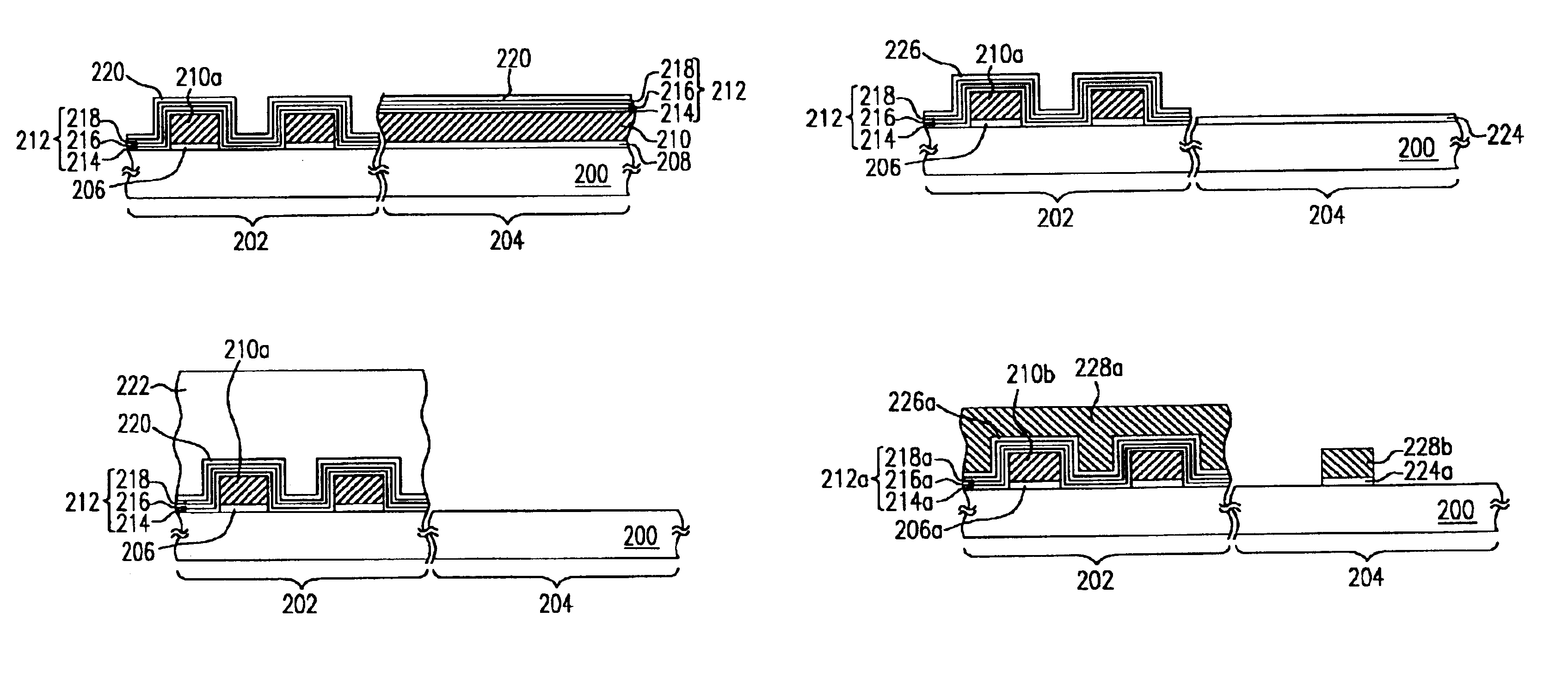
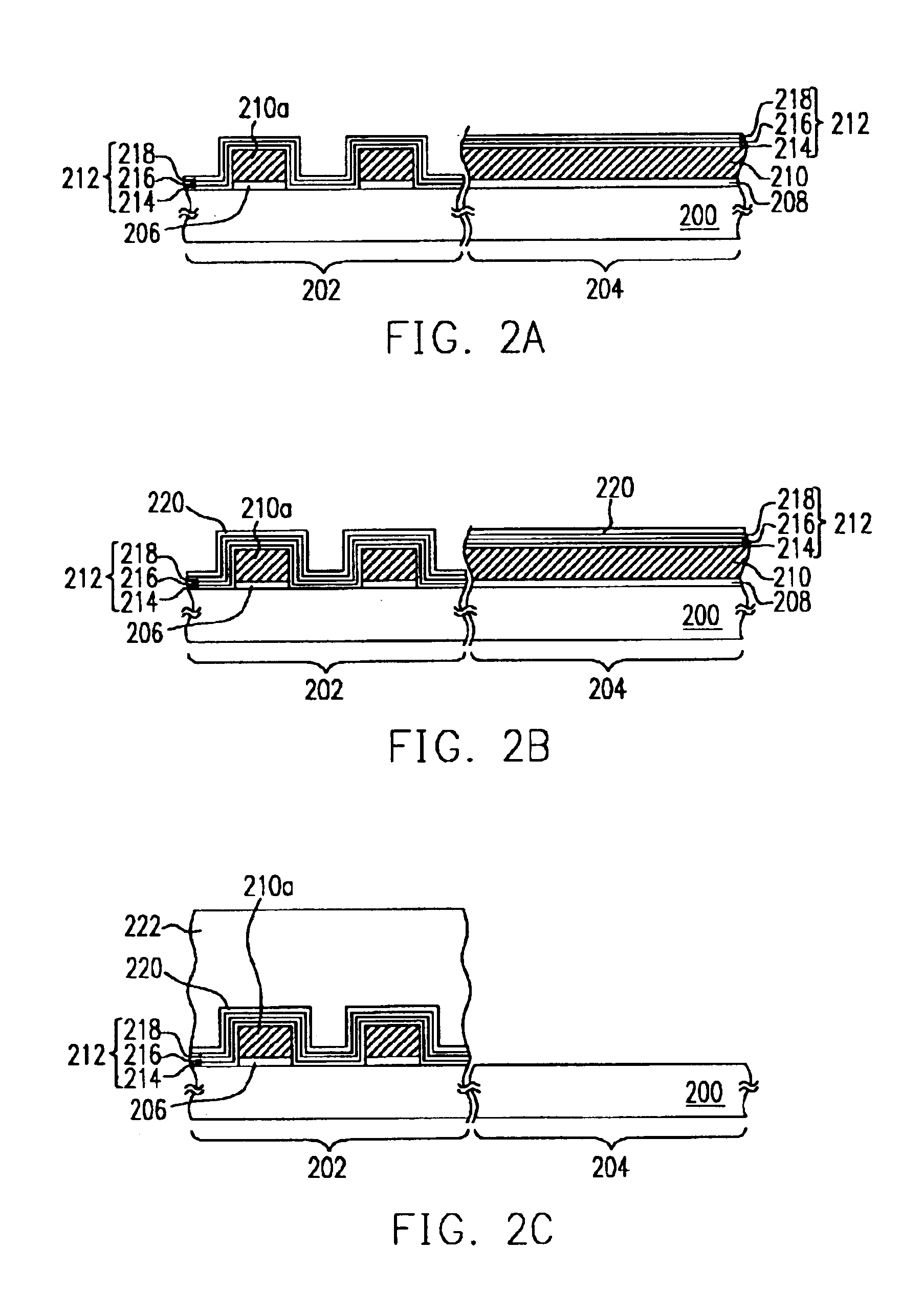
[0022]Reference will now be made in detail to the present preferred embodiments of the invention, examples of which are illustrated in the accompanying drawings. Wherever possible, the same reference numbers are used in the drawings and the description to refer to the same or like parts.

[0023]FIGS. 2A to 2F are schematic cross-sectional views showing the progression of steps for fabricating a flash memory device according to one preferred embodiment of this invention. The substrate 200 in FIGS. 2A to 2F is partitioned into two regions, a memory cell region 202 and a peripheral circuit region 204.

[0024]First, as shown in FIG. 2A, a tunnel dielectric layer 206 is formed over the memory cell region 202 and a liner layer 208 is formed over the peripheral circuit region 204. The tunnel dielectric layer and the liner layer are oxide layers formed, for example, by performing a thermal oxidation process. Thereafter, a conductive layer 210 is formed over the entire substrate 200. The conduct...


PUM


Abstract

A method of fabricating a flash memory device is provided. First, a substrate partitioned into a memory cell region and a peripheral circuit region is provided. A tunnel dielectric layer is formed over the memory cell region and a liner layer is formed over the peripheral circuit region. Thereafter, a patterned gate conductive layer is formed over the substrate. An inter-gate dielectric layer and a passivation layer are sequentially formed over the substrate. The passivation layer, the inter-gate dielectric layer, the gate conductive layer and the liner layer over the peripheral circuit region are removed. A gate dielectric layer is formed over the peripheral circuit region while the passivation layer over the memory cell region is converted into an oxide layer. Another conductive layer is formed over the substrate. The conductive layer, the oxide layer, the inter-gate dielectric layer and the gate conductive layer over the memory cell region are patterned to form a memory gate. The second conductive layer over the peripheral circuit region is similarly patterned to form a gate.

Description

BACKGROUND OF INVENTION[0001]1. Field of Invention[0002]The present invention relates to a method of manufacturing a semiconductor device. More particularly, the present invention relates to a method of manufacturing a flash memory.[0003]2. Description of Related Art[0004]Flash memory is a memory device that allows multiple data reading, writing and erasing operations. In addition, the stored data will be retained even after power to the device is turned off. With these advantages, it has been broadly applied in personal computer and electronic equipment.[0005]A typical flash memory device has a floating gate and a control gate fabricated using doped polysilicon. The control gate is set up above the floating gate with an inter-gate dielectric layer separating the two. Furthermore, a tunneling oxide layer is also set up between the floating gate and an underlying substrate (the so-called stack gate flash memory). Electric charges are injected into or drained away from the floating ga...

Claims


Application Information

Patent Timeline
IPC IPC(8): H01L21/02H01L21/336H01L21/8246H01L27/105
CPCH01L27/105H01L27/11573H01L27/11568H10B43/40H10B43/30
Inventor CHEN, KUANG-CHAOSHIH, HSUEH-HAOYANG, LING-WUU
Owner MACRONIX INT CO LTD
Why Eureka
Try Eureka