EEPROM with source line voltage stabilization mechanism

a voltage stabilization mechanism and source line technology, applied in semiconductor devices, instruments, electrical equipment, etc., can solve the problems of reducing the duration of batteries used in digital products, decelerating programming speed, and very high power consumption of prior art nand type eeprom b>10/b>, etc., to prolong the duration of batteries of portable electric equipment

Inactive Publication Date: 2005-05-03
POWERCHIP SEMICON CORP
View PDF3 Cites 36 Cited by
  • Summary
  • Abstract
  • Description
  • Claims
  • Application Information

AI Technical Summary

Benefits of technology

[0008]Accordingly, it is the primary objective of the claimed invention to provide a low-energy consumption nonvolatile memory, which is operated at relatively low voltages, thereby prolonging duration of batteries of portable electric apparatuses.
[0009]It is another objective of the claimed invention to provide an electrically erasable programmable read-only memory (EEPROM) that occupies smaller chip area and can be operated by using a reliable operation mode without the fear of over-erasing.
[0015]According to one preferred embodiment of the claimed invention, the deeply doped source well of first conductivity type serves as the source of the memory transistor. The source line is electrically coupled to the cell N well to avoid large read current bounce or potential power crash during read operations. According to another preferred embodiment of the claimed invention, the memory cell block further comprises a selection transistor having one end serially connected to the source of the memory transistor and the deeply doped source well serves as a source of the selection transistor. According to yet another embodiment of the claimed invention, each of the memory cell blocks comprises a plurality of memory transistors serially connected to each other to form a NAND memory cell array.

Problems solved by technology

However, the above-mentioned flash memory architecture has a drawback in that it consumes a great deal of electricity during a data program operation, leading to a decreased duration of batteries used in digital products.
Consequently, the prior art NAND type EEPROM 10 has very high power consumption.
Furthermore, since high voltages, for example, 20V (for the selected cell) and 12V (for non-selected cells), are required to be applied on the selected and un-selected word lines, the programming speed is decelerated, and corresponding reliability problems such as junction breakdown or over-erase will occur.
Moreover, since the operation mode of the prior art NAND flash is different from the operation mode of conventional NOR flash, it is difficult to integrate both types of memories onto a single chip.
In addition, the prior art flash memory occupies more chip area, thus more costly.

Method used


Image

  • EEPROM with source line voltage stabilization mechanism
  • EEPROM with source line voltage stabilization mechanism
  • EEPROM with source line voltage stabilization mechanism

Examples


Embodiment Construction

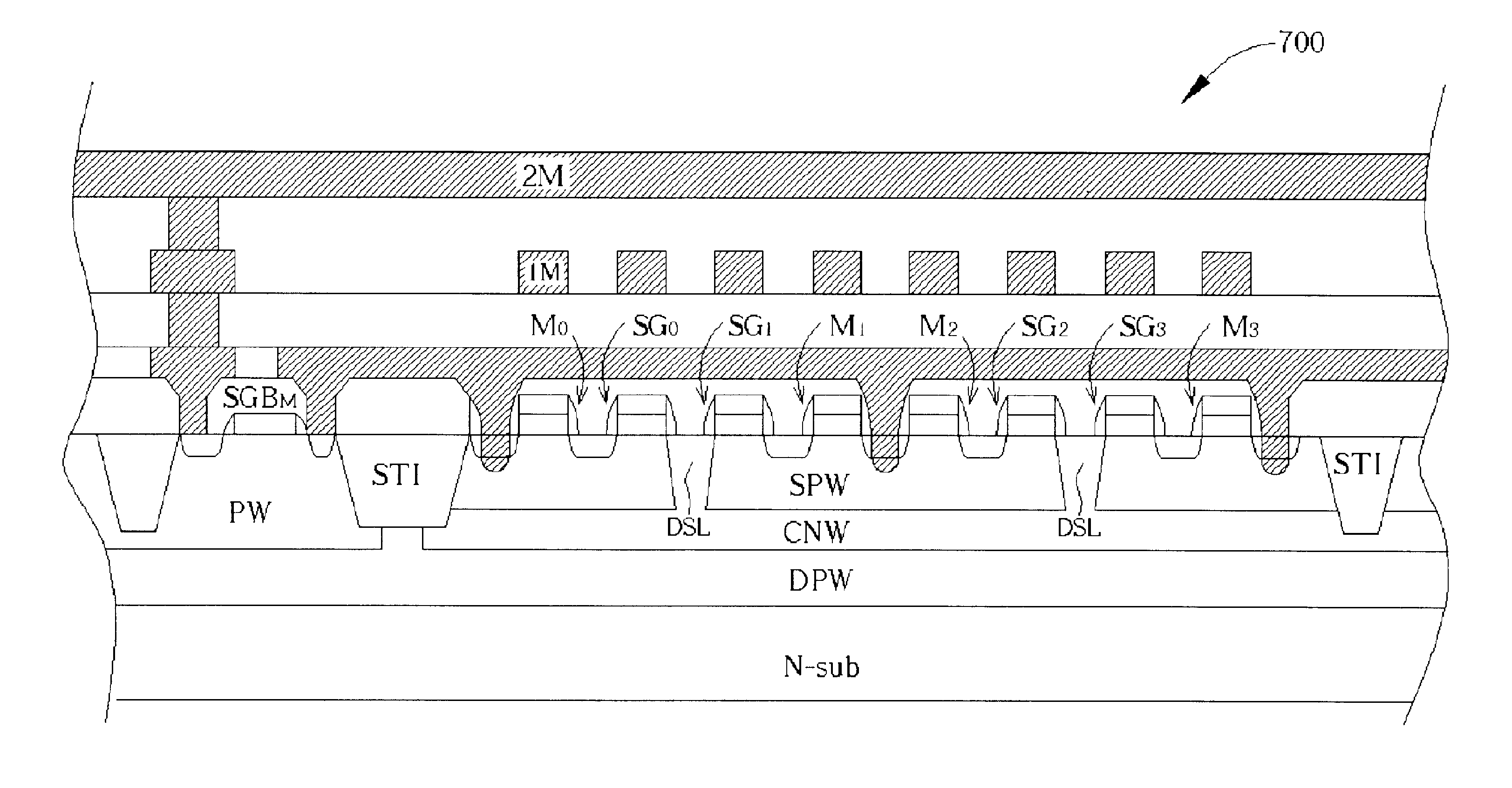
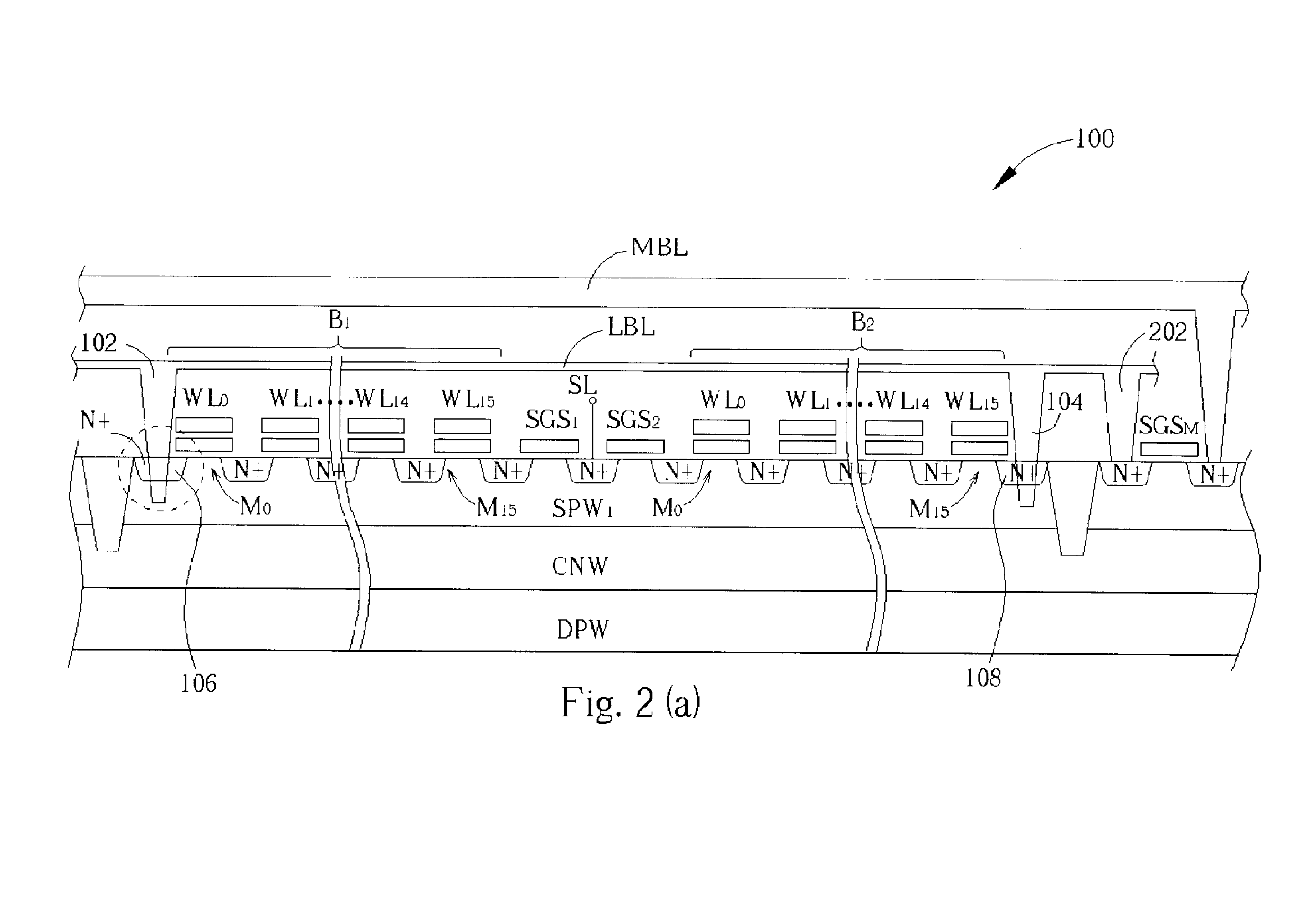
[0036]Referring to FIG. 2(a), a portion of an EEPROM 100 is shown in a cross-sectional view according to the first preferred embodiment of this invention in which only two series connected NAND memory cell blocks B1 and B2 are illustrated for the sake of simplicity. As shown in FIG. 2(a), the EEPROM 100, which is based on a novel low-voltage bi-directional FN write / erase NAND type flash memory array architecture, comprises a deep P-well (hereinafter referred to as “DPW”), a cell N-well (hereinafter referred to as “CNW”), a plurality of columns of shallow P-wells (hereinafter referred to as “SPW”). Each of the plural columns of shallow P-wells, which serve as a buried local bit line during operations, is isolated from each other with shallow trench isolation (STI) regions, which are not explicitly denoted in FIG. 2(a). To isolate the shallow P-wells from each other, the thickness of the STI layer is greater than the well depth of the shallow P-wells. It is understood that only one of...


PUM


Abstract

A low-voltage nonvolatile memory array includes an N type semiconductor substrate having a memory region. A deep P well is formed in the semiconductor substrate. A cell N well is located within the memory region in the semiconductor substrate. The cell N well is situated above the deep ion well. A shallow P well serving as a buried bit line is doped within the cell ion well. The shallow P well is isolated by an STI layer, wherein the STI layer has a thickness greater than a well depth of the shallow ion well. At least one memory transistor with a stacked gate, a source, and a drain is formed on the shallow ion well. The source of the memory transistor is electrically coupled to the cell N well to induce a capacitor between the cell N well and the deep P well during a read operation, thereby avoiding read current bounce or potential power crash. A bit line overlies the memory transistor and is electrically connected to the drain of the memory transistor via a bit line contact plug short-circuiting the drain of the memory transistor and the shallow P well.

Description

CROSS REFERENCE TO RELATED APPLICATIONS[0001]This application is a continuation in part of commonly owned, U.S. patent application Ser. No. 10 / 065,591, “BI-DIRECTIONAL FOWLER-NORDHEIM TUNNELING FLASH MEMORY”, by Ching-Sung Yang, Shih-Jye Shen, and Ching-Hsiang Hsu, filed Oct. 31, 2002 now abandoned.BACKGROUND OF INVENTION[0002]1. Field of the Invention[0003]The present invention relates to a nonvolatile semiconductor memory, and more particularly, to a bi-directional Fowler-Nordheim (FN) write / erase flash memory utilizing a compatible and low-electric consumption operation mode. An induced capacitor is created between a cell N well and an underlying deep P well to help stabilize source line voltage during read operations. According to the present invention, high-speed code flash memory and high-density data flash memory can be integrated on a single chip.[0004]2. Description of the Prior Art[0005]Recently, flash electrically erasable programmable read-only memories (EEPROMs) have ga...

Claims


Application Information

Patent Timeline
Patent Type & Authority Patents(United States)
IPC IPC(8): H01L27/115H01L21/70H01L29/66H01L21/8247H01L29/788G11C16/04
CPCH01L29/7883H01L27/11521H01L27/11524H01L27/115G11C16/0433G11C16/0483H10B41/35H10B69/00H10B41/30
Inventor YANG, CHING-SUNGSHEN, SHIH-JYEHSU, CHING-HSIANG
Owner POWERCHIP SEMICON CORP
Why Eureka
Try Eureka