Built-up bump pad structure and method for same

a technology of built-up bumps and bumps, which is applied in the direction of manufacturing tools, sustainable manufacturing/processing, and final product manufacturing, etc., can solve the problems of increasing the stress level at the connection between the solder bump and the die, affecting the production yield, and the chip stand-off height is decreased, so as to reduce the thickness of the solder mask, reduce the stress level, and improve the production yield

Inactive Publication Date: 2005-05-03
TEXAS INSTR INC
View PDF7 Cites 139 Cited by
  • Summary
  • Abstract
  • Description
  • Claims
  • Application Information

AI Technical Summary

Benefits of technology

[0005]Technical advantages of particular embodiments of the present invention include a bump pad structure that reduces the thickness of the solder mask above the bump pad. This reduction in the height of the solder mask above the bump pad allows for the use of fine pitch bump pads which are less sensitive to assembly tolerances, and, therefore, result in higher production yields.
[0006]Another technical advantage of particular embodiments of the present invention is the ability to standardize substrates having different assembly tolerances for use in manufacturing flip chips. This may be accomplished by building up the bump pad structures of the substrates as needed, until all the substrates have similar assembly tolerances. This allows substrates supplied by different manufacturers having different tolerances to be used in the same flip chip assembly, regardless of their original tolerances.
[0007]Yet another technical advantage of particular embodiments of the present invention is a bump pad structure that can be used with low-cost, photo-imageable substrate materials, which helps reduce flip chip manufacturing costs and production times.
[0008]Still another technical advantage of particular embodiments of the present invention is the ability to increase the stand-off height of the flip chip assembly. By attaching the solder bumps connecting the die and substrate to the larger bump pad structures, the solder bumps are effectively seated higher on the substrate. This increases the stand-off height of the flip chip, helping to reduce the stress on the solder joints due to any difference in CTE between the die and the substrate, and improving the reliability of the flip chip assembly.

Problems solved by technology

This typically results in the flip chip having a decreased stand-off height between the die and the substrate, which may increase the level of stress at the connection between the solder bumps and the die due to the differences in the coefficients of thermal expansion (CTE) of the die and substrate.
Additionally, shrinking chip sizes have lead to increasingly tighter assembly tolerances, which can negatively impact production yields and make it difficult to interchangeably use substrates from different manufacturers that may have different tolerances.

Method used


Image

  • Built-up bump pad structure and method for same
  • Built-up bump pad structure and method for same

Examples


Embodiment Construction

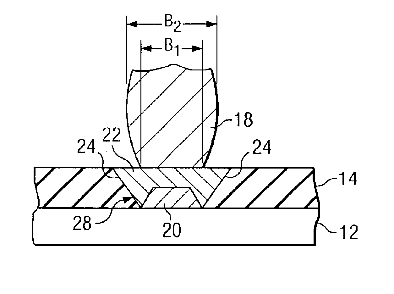
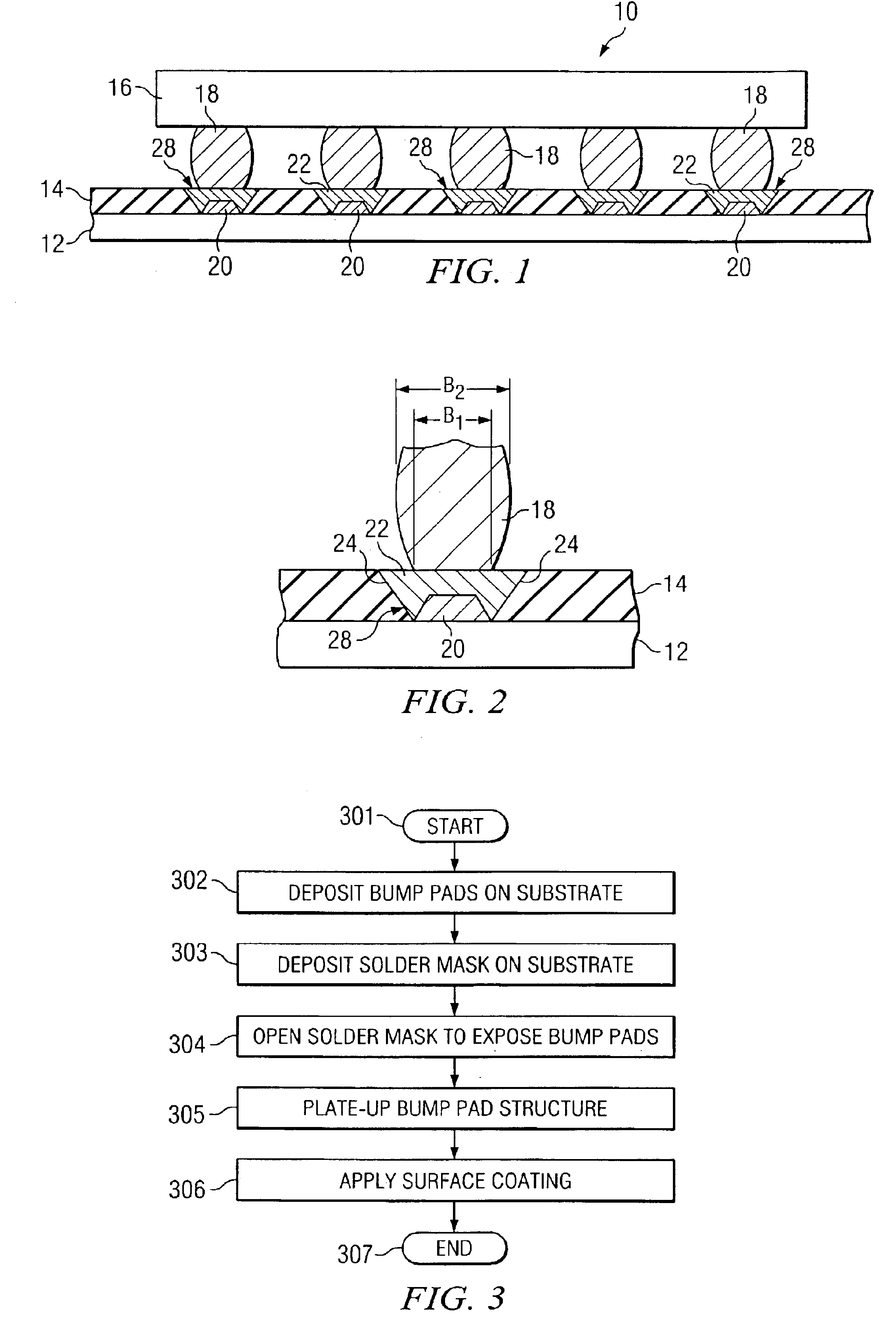
[0014]FIG. 1 illustrates flip chip assembly 10 in accordance with a particular embodiment of the present invention. Flip chip assembly 10 is a flip chip in which a conductive material has been deposited on each of the bump pads on the surface of the substrate, at least partially filling the opening in the solder mask around each bump pad. This conductive material increases the height of the bump pad structure, which in turn increases the stand-off height of flip chip assembly 10. The addition of the conductive material also reduces the thickness of the solder mask above the bump pad structure, which results in the flip chip assembly being less sensitive to assembly tolerances. Additionally, substrates having differing tolerances may be standardized by adding conductive material to the bump pad structures as needed until all the substrates share a common tolerance level.

[0015]As shown in FIG. 1, flip chip assembly 10 includes die 16 and substrate 12, which are positioned generally pa...


PUM

PropertyMeasurementUnit
conductiveaaaaaaaaaa
heightaaaaaaaaaa
sizesaaaaaaaaaa

Abstract

In accordance with the present invention, a built-up bump pad structure and method for the same are provided. The bump pad structure includes a substrate, a bump pad disposed upon the substrate, a solder mask disposed upon the substrate defining an opening around the bump pad, and a conductive material deposited upon the bump pad such that the conductive material at least partially fills the opening around the bump pad.

Description

TECHNICAL FIELD OF THE INVENTION[0001]The present invention relates in general to semiconductor manufacturing and, in particular, to a built-up bump pad structure and method for the same.BACKGROUND OF THE INVENTION[0002]Flip chips are microelectronic devices in which a silicon chip, or die, is attached facedown to a substrate via a plurality of small solder bumps. In general, a die attach system “picks and flips” the die directly from a silicon wafer and places the die on the substrate using a plurality of solder bumps to form an electrical connection with a plurality of bump pads on the surface of the substrate. Once the solder has been reflowed and solidified, a non-conductive underfill material is typically inserted into the gap between the die and substrate to strengthen the connection between the two and to provide a barrier to moisture or other contaminants.[0003]As chip sizes have decreased over time, flip chip assemblies have also decreased in size. These smaller chip sizes ...

Claims


Application Information

Patent Timeline
Patent Type & Authority Patents(United States)
IPC IPC(8): H01L23/48H01L23/498H05K3/24H05K1/11H05K3/34
CPCH01L23/49811H05K1/111H05K3/243H01L2224/16225H01L2924/01078H01L2924/01079H05K3/245H01L2924/10253H05K3/3452H05K2201/035H01L2924/01322H01L2924/00H01L2224/16237H01L2924/00014Y02P70/50H01L2224/0401
Inventor MURTUZA, MASOODVENKATESWARAN, MUTHIAHCHAUHAN, SATYENDRA SINGH
Owner TEXAS INSTR INC
Why Eureka
Try Eureka