SiC single crystal, method for manufacturing SiC single crystal, SiC wafer having an epitaxial film, method for manufacturing SiC wafer having an epitaxial film, and SiC electronic device

Inactive Publication Date: 2005-05-10
DENSO CORP +1
View PDF5 Cites 19 Cited by
  • Summary
  • Abstract
  • Description
  • Claims
  • Application Information

AI Technical Summary

Benefits of technology

[0028]A thirteenth aspect of the present invention is an SiC electronic device that is formed using the SiC wafer having the epitaxial film that is described in the twelfth aspect of the present invention. The SiC wafer having the epitaxial film includes a relatively small

Problems solved by technology

However, according to study reports to date, it is thought that crystal imperfections in the SiC single crystal such as a micropipe defect, a screw dislocation, an edge dislocation, and a stacking fault are the causes of the leak current and the breakdown voltage lowering in

Method used


Image

  • SiC single crystal, method for manufacturing SiC single crystal, SiC wafer having an epitaxial film, method for manufacturing SiC wafer having an epitaxial film, and SiC electronic device
  • SiC single crystal, method for manufacturing SiC single crystal, SiC wafer having an epitaxial film, method for manufacturing SiC wafer having an epitaxial film, and SiC electronic device
  • SiC single crystal, method for manufacturing SiC single crystal, SiC wafer having an epitaxial film, method for manufacturing SiC wafer having an epitaxial film, and SiC electronic device

Examples


first embodiment

[0049

[0050]As shown in FIGS. 1 to 3, a refined SiC single crystal and an SiC seed crystal for making the refined SiC single crystal are formed in a first embodiment. The method for forming the refined SiC single crystal and the seed crystal includes N steps of growth, and each growth step is expressed in an n growth step, in which n is an ordinal number corresponding to a natural number from one to N.

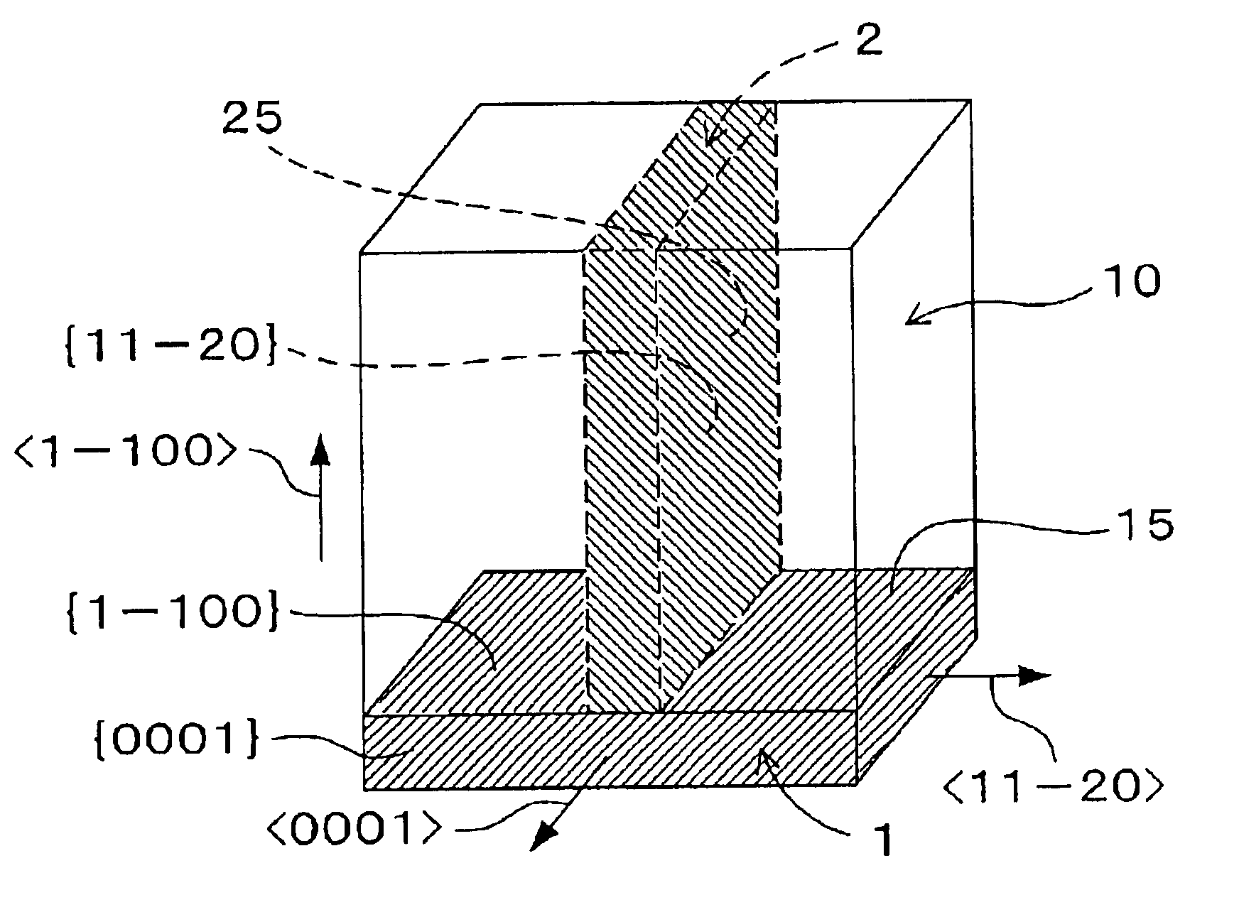
[0051]An example of the method, in which N=3, is as follows. As shown in FIG. 1, at a first growth step, i.e., at n=1, a first seed crystal 1, in which a plane having an inclination of 20 degrees or smaller from a {1-100} plane or an inclination of 20 degrees or smaller from a {11-20} plane is exposed as a first growth surface 15, is used, and a first grown crystal 10 is formed by growing an SiC single crystal on the first growth surface 15. The first growth surface 15 is preferably the {1-100} plane or the {11-20} plane. In that case, the first grown crystal 10 is formed in a directio...

second embodiment

[0069

[0070]A second embodiment is a method for forming a refined SiC single crystal and an SiC seed crystal that is used to make the refined SiC single crystal. The method includes an intermediate growth step, at which a {0001}-plane growth is carried out, in addition to the first growth step, the intermediate growth step, and the final growth step described in the first embodiment. Specifically, at the intermediate growth step including the {0001}-plane growth, an n seed crystal is formed such that a plane having an inclination of 20 degrees or smaller from a {0001} plane of an (n−1) crystal is exposed as an n growth surface, and an SiC single crystal is grown on the n growth surface.

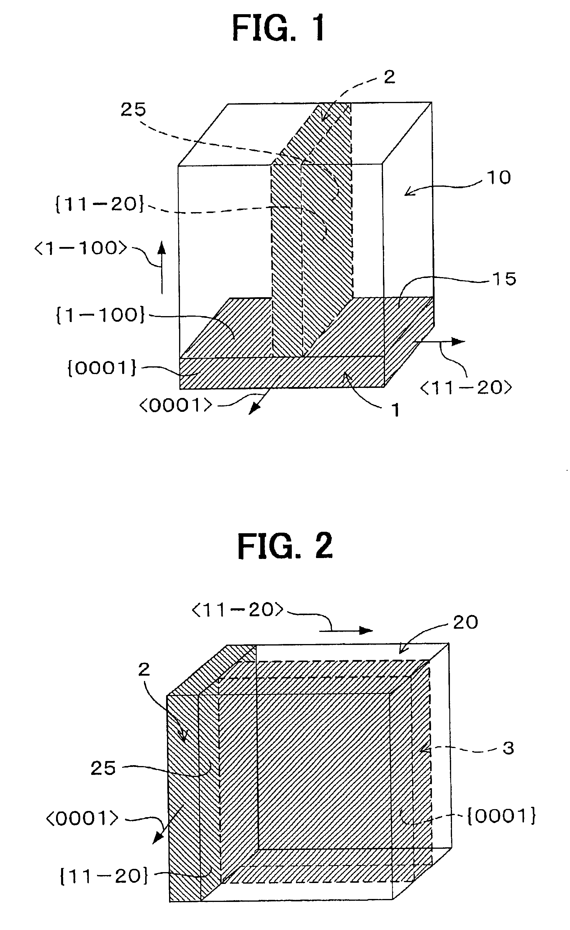
[0071]An example of the method is as follows. A first growth step is carried out in the same manner as described in the first embodiment. Then, a second seed crystal 2 is formed at a second growth step such that a second growth surface 25 is a {11-20} plane, which has an inclination of 90 degrees from ...

third embodiment

[0074

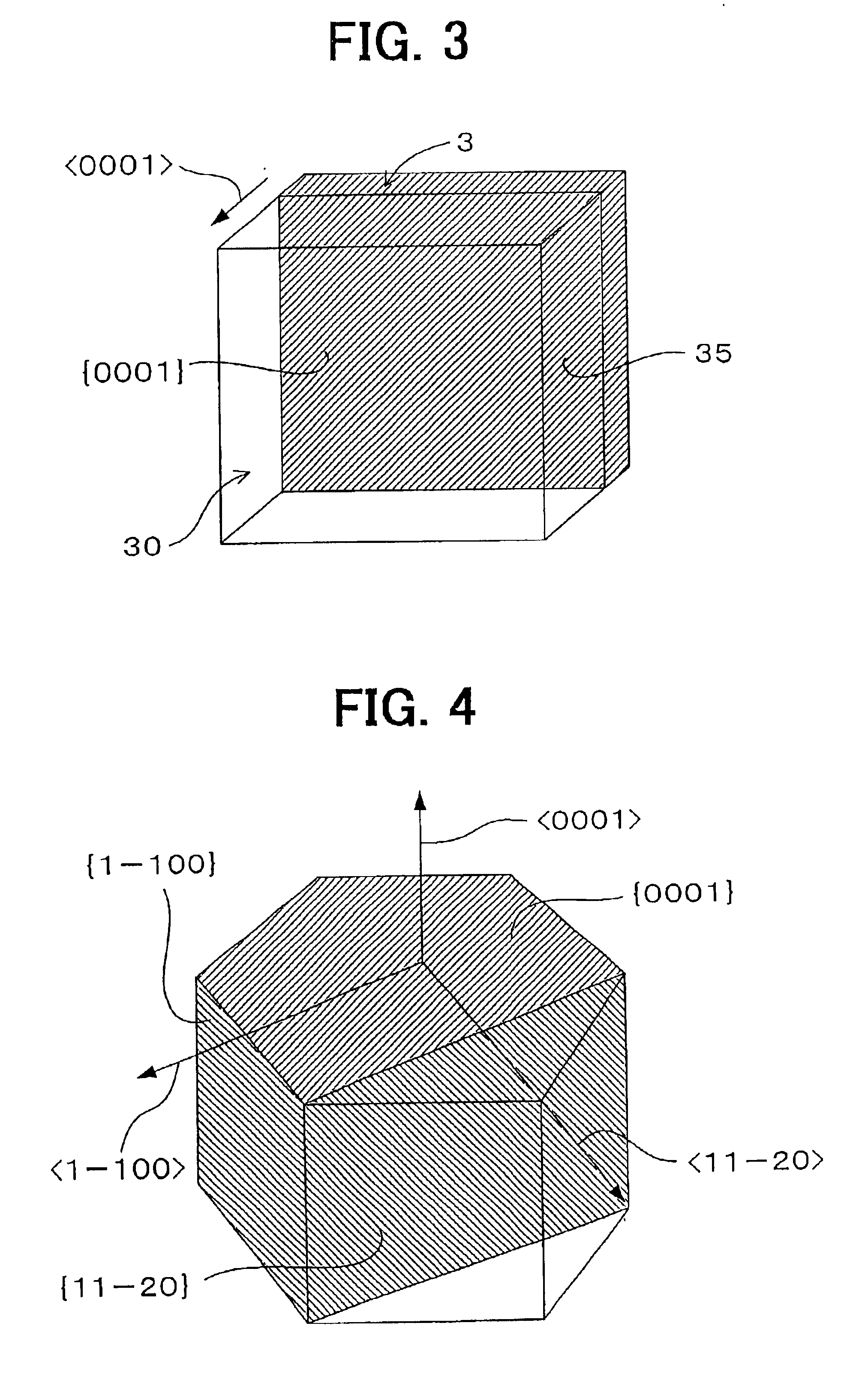
[0075]A third embodiment is the same as the first embodiment except that each SiC single crystal 10, 20, 30 is grown on each growth surface 15, 25, 35 by a chemical vapor deposition (CVD). In the first embodiment, sublimation-reprecipitation technique is used for growing an SiC single crystal on each seed crystal. However, the method that can be used for growing the SiC single crystal in the present invention is not limited to sublimation-reprecipitation technique. Any method that enables to grow a single crystal ingot with sufficient growth height may be applied. In the third embodiment, each SiC single crystal 10, 20, 30 is grown on each growth surface 15, 25, 35 by a CVD, in which a mixture of silane (SiH4) gas and propane (C3H8) gas is used as a raw material gas containing silicon (Si) and carbon (C).

[0076]With a growth using the CVD, it is possible to provide a quality SiC single crystal that includes a relatively small number of micropipe defects, dislocations, and so on....


PUM


Abstract

A refined SiC single crystal that includes a small number of defects is provided as follows. At a first growth step, a first seed crystal is formed from a crude SiC single crystal, and a first grown crystal is formed on a first growth surface, which is a plane having an inclination of 20 degrees or smaller from a {1-100} plane or an inclination of 20 degrees or smaller from a {11-20} plane. At an intermediate growth step, an n growth crystal is formed on an n growth surface, which is a plane having an inclination of 45 to 90 degrees from an (n−1) growth surface and an inclination of 60 to 90 degrees from a {0001} plane. At a final growth step, a final SiC single crystal is formed on a final growth surface, which has an inclination of 20 degrees or smaller from a {0001} plane.

Description

CROSS REFERENCE TO RELATED APPLICATION[0001]This application is based on and incorporates herein by reference Japanese Patent Applications No. 2001-315367 filed on Oct. 12, 2001, No. 2002-80295 filed on Mar. 22, 2002, and No. 2002-128725 filed on Apr. 30, 2002.BACKGROUND OF THE INVENTION[0002]The present invention relates to an SiC single crystal including a relatively small number of dislocations and defects and a method for manufacturing the SiC single crystal, to an SiC wafer having an epitaxial film and a method for manufacturing the SiC wafer, and to an SiC electronic device, in which the SiC wafer is used.[0003]Nowadays, an SiC semiconductor utilizing an SiC single crystal is expected to become a candidate material for next generation's power device substituting an Si semiconductor. However, according to study reports to date, it is thought that crystal imperfections in the SiC single crystal such as a micropipe defect, a screw dislocation, an edge dislocation, and a stacking ...

Claims


Application Information

Patent Timeline
IPC IPC(8): C30B25/00C30B25/18C30B23/00C30B33/00C30B25/20
CPCC30B23/00C30B25/00C30B25/20C30B33/00C30B29/36H01L2924/0002H01L2924/00
Inventor NAKAMURA, DAISUKEITO, TADASHIKONDO, HIROYUKINAITO, MASAMI
Owner DENSO CORP
Why Eureka
Try Eureka