Multistage tunable gain optical amplifier

a multi-stage, optical amplifier technology, applied in the structure of semiconductor amplifiers, semiconductor lasers, semiconductor lasers, etc., can solve the problems of degrading the corresponding signal-to-noise ratio, attenuating the optical signal, and affecting etc., to achieve a higher saturable power, improve noise performance, and improve the overall amplification of optical amplifiers

Inactive Publication Date: 2005-05-10
II VI DELAWARE INC
View PDF26 Cites 10 Cited by
  • Summary
  • Abstract
  • Description
  • Claims
  • Application Information

AI Technical Summary

Benefits of technology

[0018]In accordance with the present invention, a multi-stage tunable gain optical amplifier device for amplifying an optical signal includes at least two optical amplifier stages coupled in series. In an embodiment, one of the optical amplifier stages comprises a gain medium having an amplifying path for amplifying an optical signal. The second optical amplifier stage is a tunable-gain lasing semiconductor optical amplifier (SOA) stage comprising a semiconductor gain medium having an amplifying path for amplifying an optical signal propagating along the amplifying path and a laser cavity. The laser cavity is pumped above a lasing threshold to clamp the gain of the semiconductor gain medium to a constant value. The overall gain of the tunable-gain lasing SOA stage is tunable.
[0020]In another embodiment of the invention, a third optical amplifier stage is added to the multi-stage tunable gain optical amplifier described above. In this embodiment, the first optical amplifier stage is designed to provide good noise performance. The third optical amplifier stage is designed to produce a high output power. The tunable-gain optical amplifier stage allows the overall gain of the multi-stage tunable gain optical amplifier to be tuned by adjusting the gain value of the tunable gain optical amplifier stage.
[0022]The present invention is particularly advantageous because varying the noise figure and saturable power from stage to stage, results in better noise performance and higher saturable power for the multi-stage tunable gain optical amplifier than is possible in a single stage optical amplifier providing the same output power. In addition, since one of the optical amplifier stages is capable of adjusting the gain of that stage, the overall amplification of optical amplifier is tunable.

Problems solved by technology

As another example, phenomena such as fiber losses, losses due to insertion of components in the transmission path, and splitting of the optical signal may attenuate the optical signal and degrade the corresponding signal-to-noise ratio as the optical signal propagates through the communications system.
Conventional optical amplifiers, however, suffer from various drawbacks.
One drawback of fiber amplifiers is that they typically can only operate over a narrow wavelength range when multiple fiber amplifiers are cascaded.
This is especially problematic if the optical signal to be amplified covers a wide range of wavelengths, as would be the case if the entire bandwidth of the optical fiber were to be efficiently utilized.
Another disadvantage of fiber amplifiers is their transient response to channel drop-out in wavelength division multiplexing systems.
Further problems with fiber amplifiers include their relatively large size, slow switching speed, power inefficiency, difficulties in mass producing them, and their high cost which makes them prohibitively expensive for many applications.
One problem with non-lasing semiconductor optical amplifiers is that the gain depends on the amplitude of the optical signal.
This results in distortion of the optical signal and possibly also crosstalk between different optical signals propagating simultaneously through the system.
This problem is the result of gain saturation, in which there are insufficient carriers in the conduction band to provide the full amount of gain to higher power signals.
However, lasing semiconductor optical amplifiers also suffer from inherent drawbacks.
For example, there is an inherent tradeoff between noise performance and power output.
If the carrier density at the lasing threshold is high, the amplifier will have good noise performance but will have a low saturable power thus limiting its power output.
On the other hand, an amplifier with a low carrier density at the lasing threshold will be capable of large power output but suffer from poor noise performance.
This inherent tradeoff makes it difficult for a lasing semiconductor optical amplifier to attain both a low noise and a high power output.

Method used


Image

  • Multistage tunable gain optical amplifier
  • Multistage tunable gain optical amplifier
  • Multistage tunable gain optical amplifier

Examples


Embodiment Construction

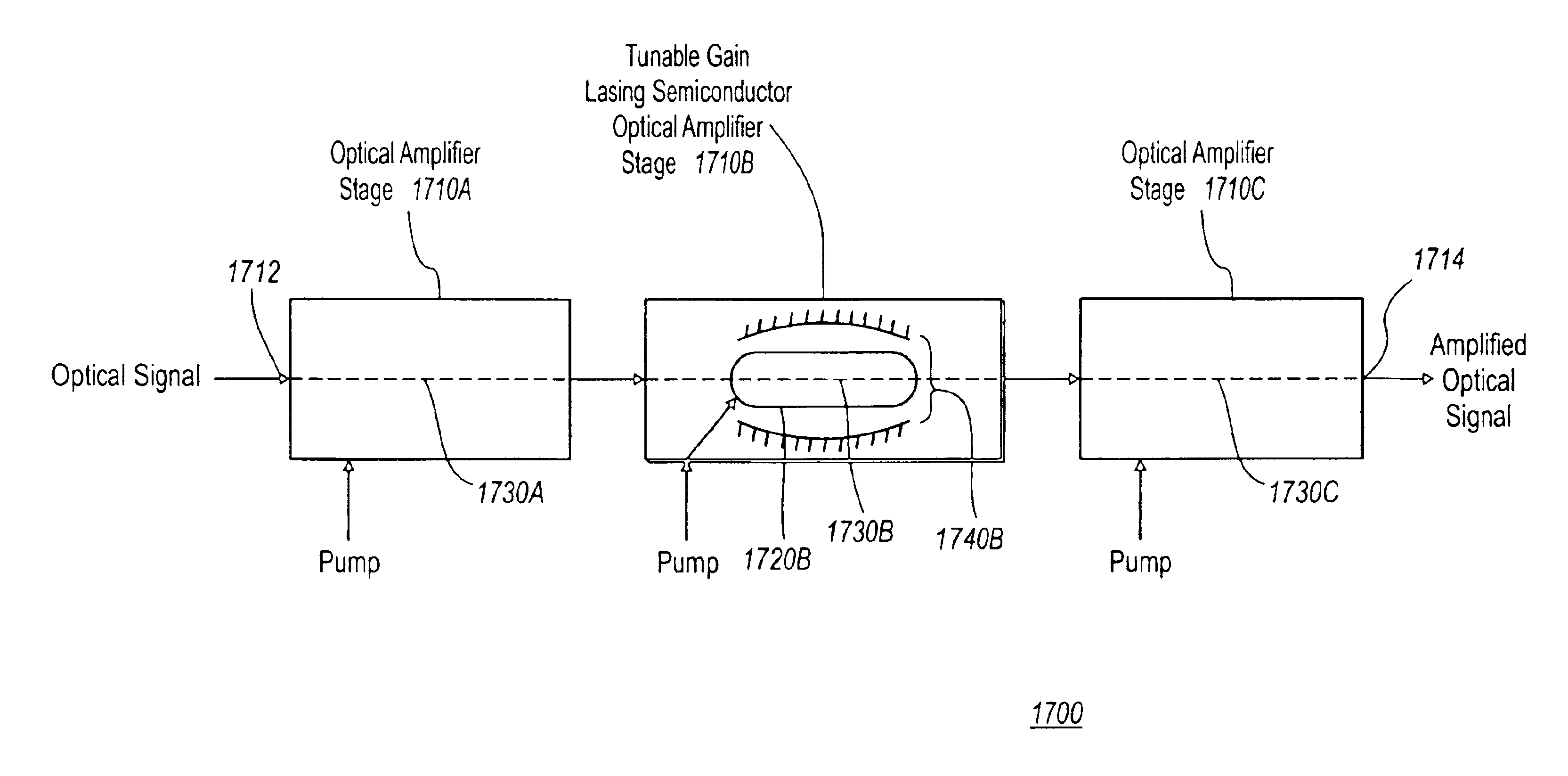
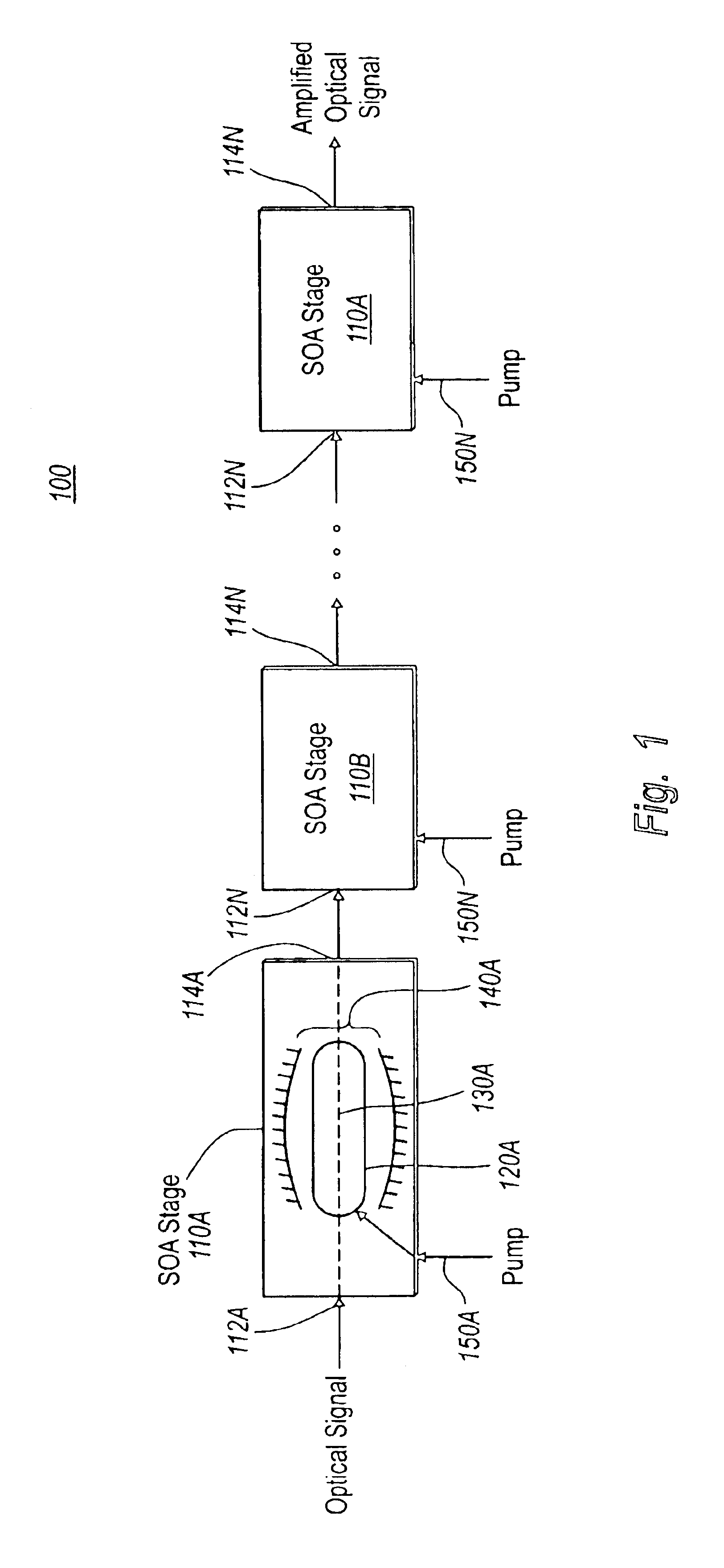
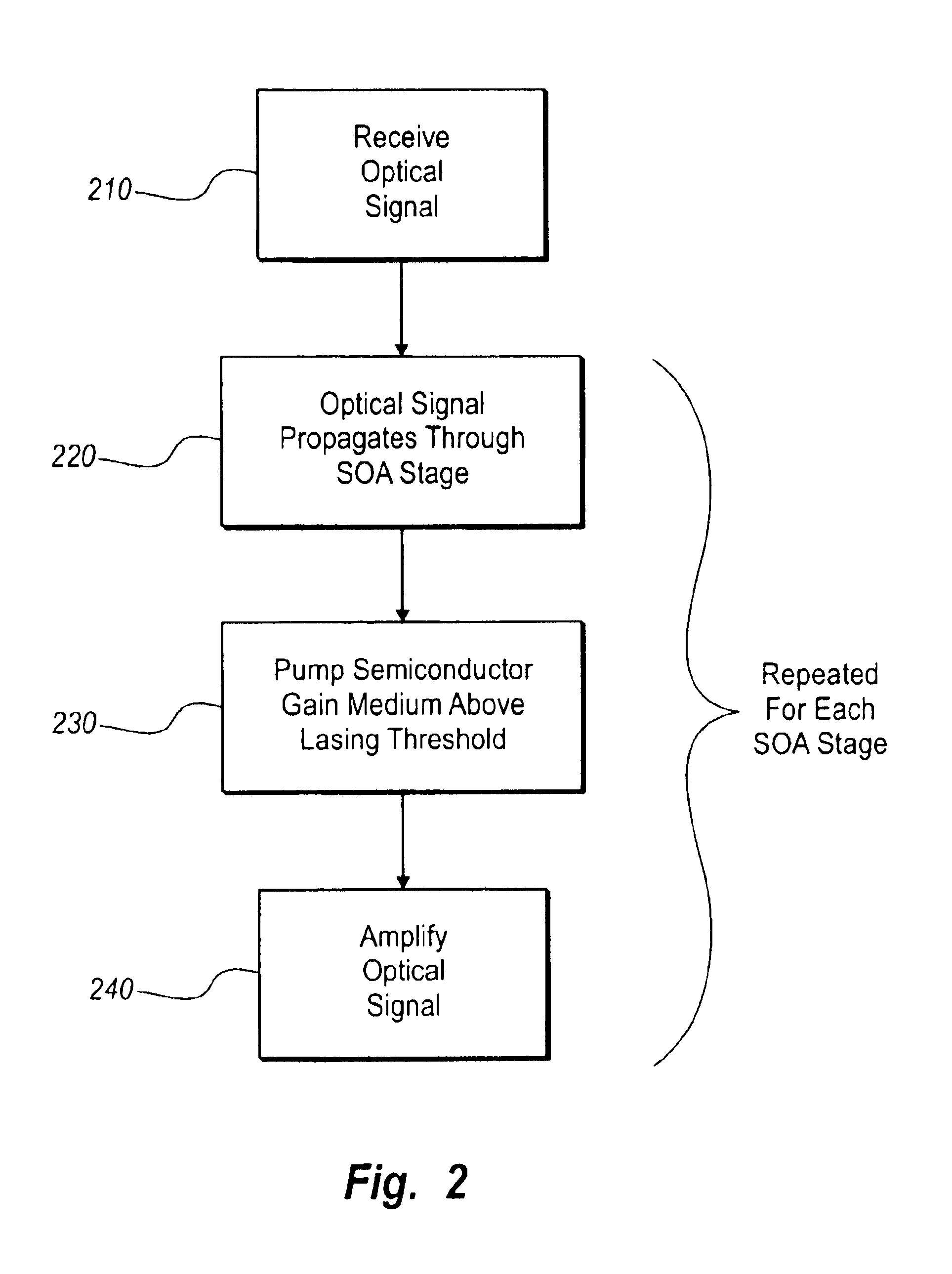
[0050]FIG. 1 is a diagram of a multi-stage lasing semiconductor optical amplifier (SOA) 100 in accordance with the present invention. The SOA 100 includes a number of SOA stages 110A-110N (collectively, SOA stages 110). Each SOA stage 110 has an input 112 and an output 114 and the SOA stages 110 are coupled in series with the output of each SOA stage 110 coupled to the input of the next SOA stage 110. As shown in the detail of SOA stage 110A, each SOA stage 110 includes a semiconductor gain medium 120, with an amplifying path 130 coupled between the input 112 and the output 114 of the SOA stage 110 and traveling through the semiconductor gain medium 120. Each SOA stage 110 further includes a laser cavity 140 including the semiconductor gain medium 120, and a pump input 150 coupled to the semiconductor gain medium 120. The pump input is for receiving a pump to pump the semiconductor gain medium 120 above a lasing threshold for the laser cavity 140. The SOA stages 110 are not identica...


PUM


Abstract

A multi-stage tunable gain optical amplifier device amplifies an optical signal by a gain amount which can be adjusted in one of the stages of the amplifier. The multi-stage amplifier includes at least two optical amplifier stages coupled in series, one of which is a tunable gain amplifier stage. The optical amplifier stages are characterized by a design parameter which varies from stage to stage. In a preferred embodiment, the design parameter includes a noise figure and a saturable power, with both parameters increasing as the optical signal propagates from stage to stage. As a result, the multi-stage tunable gain optical amplifier can achieve better noise performance and higher output power than a single stage optical amplifier with a constant noise figure and saturable power.

Description

CROSS-REFERENCE TO RELATED APPLICATIONS[0001]This application claims benefit of U.S. Provisional Patent Application Ser. No. 60 / 274,553, “Multistage, Variable Gain Optical Amplifier,” by Sol P. Dijaili and John M. Wachsman, filed Mar. 9, 2001.[0002]This application is a continuation-in-part of U.S. patent application Ser. No. 09 / 273,813, “Tunable-gain Lasing Semiconductor Optical Amplifier”, by Jeffrey D. Walker, Sol P. Dijaili and Daniel A. Francis, filed Mar. 22, 1999 now U.S. Pat. No. 6,445,495. This application is also a continuation-in-part of U.S. patent application Ser. No. 09 / 416,817, “Low-Noise, High-Power Optical Amplifier,” by Sol P. Dijaili and Jeffrey D. Walker, filed Oct. 12, 1999 now U.S. Pat. No. 6,512,629.[0003]The subject matter of all of the foregoing is incorporated herein by reference.BACKGROUND OF THE INVENTION[0004]1. Field of the Invention[0005]The present invention relates to optical communications systems and, more particularly, to optical amplifiers.[0006]...

Claims


Application Information

Patent Timeline
Patent Type & Authority Patents(United States)
IPC IPC(8): H01S5/40H01S5/50H01S5/00H01S5/183H01S5/42H01S5/06H01S5/026
CPCH01S5/0265H01S5/5027H01S5/0611H01S5/1032H01S5/18302H01S2301/02H01S5/2027H01S5/5072H01S5/18311
Inventor DIJAILI, SOL P.WACHSMAN, JOHN M.
Owner II VI DELAWARE INC
Why Eureka
Try Eureka