Back illuminated photodiodes

a photodiode and backlight technology, applied in the field of photodiodes, can solve the problems of adding significant complexity to the manufacturing process, and achieve the effect of high reflection surface and high reflection

Inactive Publication Date: 2005-05-17
LUMENTUM OPERATIONS LLC
View PDF8 Cites 26 Cited by
  • Summary
  • Abstract
  • Description
  • Claims
  • Application Information

AI Technical Summary

Benefits of technology

[0027]Advantageously, this invention provides a high reflection surface without adversely affecting the ohmic contact of metal to the semiconductor substrate; ohmic contact to the III-V semiconductor is achieved using an alloyed metal to bond and partially alloy with the semiconductor. Since the alloy is a poor light reflector a non alloyed material is provided in a central location which is highly reflecting.

Problems solved by technology

However, the intrinsic responsivity of the APD (i.e., at unity gain) is still critical to the device performance.
Furthermore, the formation of a distributed Bragg reflector between the epitaxial layer and the contact adds significant complexity to the manufacturing process.

Method used


Image

  • Back illuminated photodiodes
  • Back illuminated photodiodes
  • Back illuminated photodiodes

Examples


Embodiment Construction

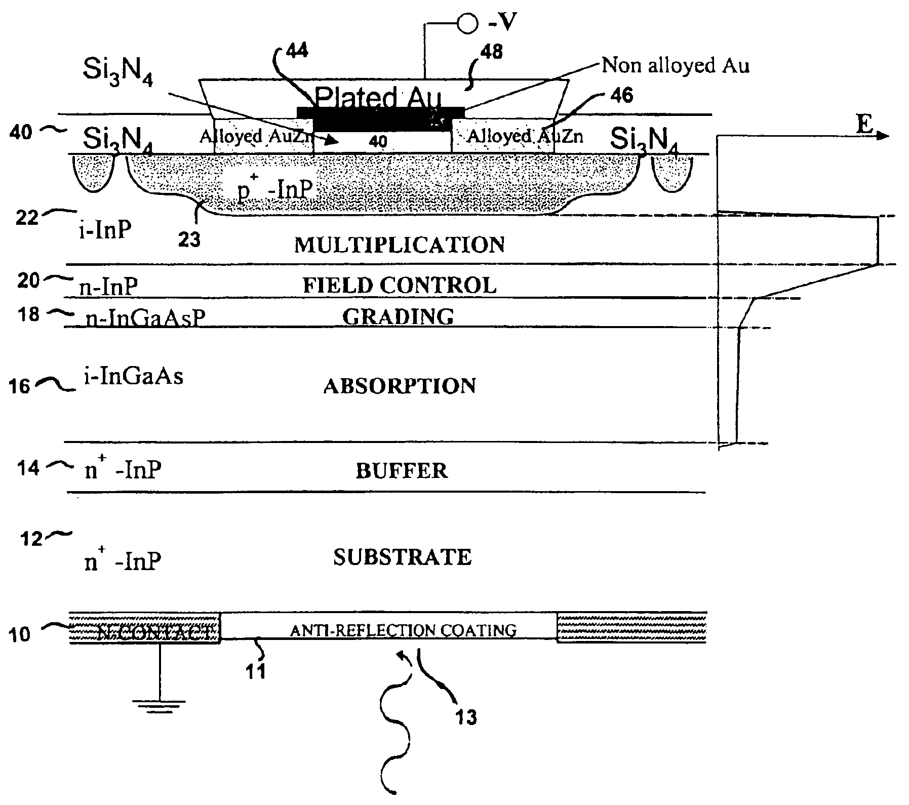
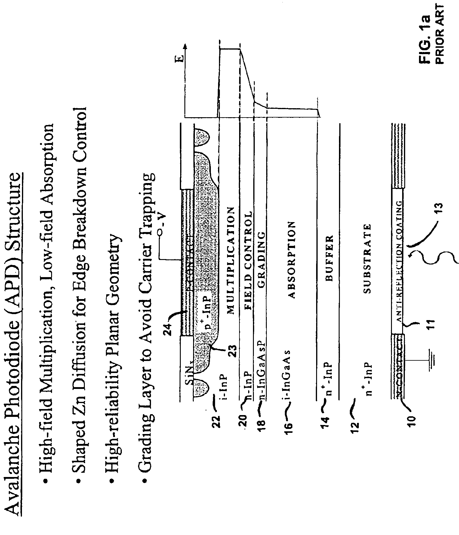
[0034]The layer structure of a prior art APD PC is shown schematically in detail in FIG. 1a. A terminal layer 10 adjoins an antireflection layer window 11 which defines a port 13 supported on the input end face of a substrate 12. A layer structure is created on the substrate including: a buffer layer 14, absorption layer 16, grading layer 18, field control layer 20, capping layer 22 and P dopant diffused region of the capping layer 23. Directly contacting the diffused region of the capping layer 23 is an alloyed material P-contact 24 creating some alloy mixing with the epitaxial ion infused capping layer 23. Alloyed contact material provides superior ohmic contact, however the reflectivity is inefficient. Alloyed AuZn has a reflectivity of approximately 45%.

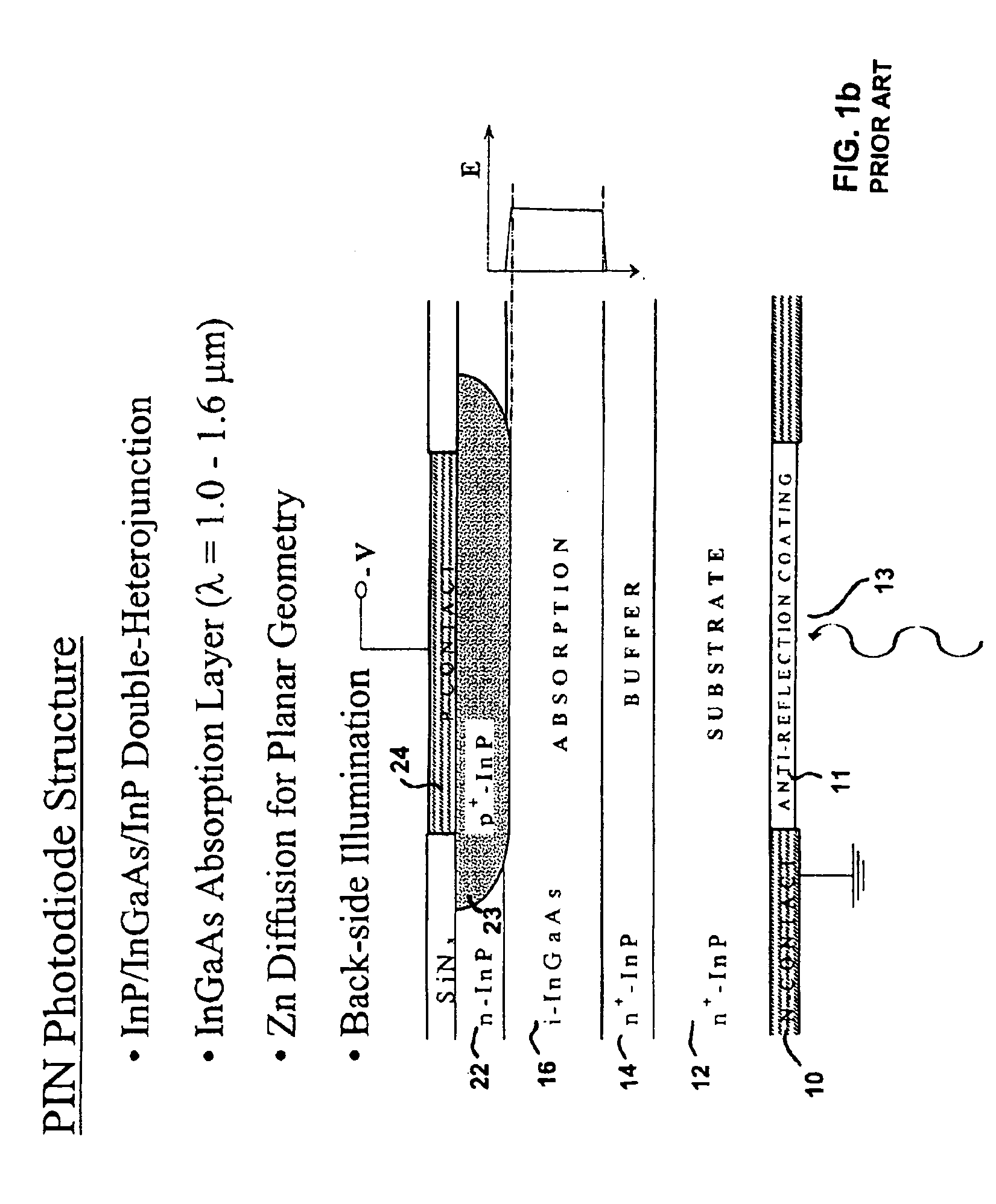
[0035]FIG. 1b illustrates a similar schematic layer structure of a prior art PIN photodiode. The N-contact 10 and anti-reflection coating 11 are provided on the N side of a substrate 12. The layer structure is somewhat simpler in...


PUM


Abstract

A highly reflecting back illuminated diode structure allows light that has not been absorbed by a semiconductor absorbing region to be back reflected for at least a second pass into the absorbing region. The diode structure in a preferred embodiment provides a highly reflecting layer of gold to be supported in part by a conducting alloyed electrode ring contact and in part by a passivation layer of SixNy. Conveniently this structure provides a window within the contact which allows light to pass between the absorbing region and the reflecting layer of gold.

Description

CROSS-REFERENCE TO RELATED APPLICATIONS[0001]This application claims priority of U.S. Provisional Patent Application No. 60 / 355,880 filed on Feb. 11, 2002, entitled “Avalanche Photodiode With Improved Responsivity Utilizing A Highly Reflective Metal Contact” which is incorporated herein by reference for all purposes.TECHNICAL FIELD[0002]The present invention relates to photodiodes(PDs) and more particularly, to diode structures applicable to back-illuminated positive-intrinsic-negative (PIN) photodiodes and avalanche photodiodes (APDs).BACKGROUND OF THE INVENTION[0003]One of the major parameters that determine the performance of a photodiode is its responsivity to light. The responsivity, R, is defined as the current generated by the photodiode (PD) per unit incident light power and is typically expressed in amperes per watt (A / W). This detection property of a PD can be equivalently described by the quantum efficiency ηext, which is 100% when every incident photon excites an electro...

Claims


Application Information

Patent Timeline
Patent Type & Authority Patents(United States)
IPC IPC(8): H01L31/102H01L31/0264H01L31/0304H01L31/103H01L31/107
CPCH01L31/0304H01L31/107H01L31/1035Y02E10/544
Inventor KWAN, STEVENBEN-MICHAEL, RAFAELITZLER, MARK
Owner LUMENTUM OPERATIONS LLC
Why Eureka
Try Eureka