Booster circuit for non-volatile semiconductor memory device

a voltage generation circuit and non-volatile technology, applied in semiconductor devices, solid-state devices, instruments, etc., can solve the problem of difficulty in setting the boosted voltage hv equal to the standby voltage, and achieve the effect of eliminating the parasitic capacitance, increasing the boosted voltage, and effectively interfering with the reference voltage increas

Inactive Publication Date: 2005-05-31
SEIKO EPSON CORP
View PDF14 Cites 19 Cited by
  • Summary
  • Abstract
  • Description
  • Claims
  • Application Information

AI Technical Summary

Benefits of technology

[0033]The advantage of the present invention is thus to solve the problems of the prior art technique discussed above and to provide a booster circuit for a non-volatile semiconductor memory device, which desirably eliminates the effects of a parasitic capacitance and effectively interferes with an increase in reference voltage accompanied by an increase in boosted voltage.
[0034]In order to attain at least part of the above and the other related objects, the present invention is directed to a booster circuit applied for a non-volatile semiconductor memory device, which includes a memory cell array of multiple non-volatile memory elements and has an operation mode including at least a standby mode to stand ready for an access to one of the multiple non-volatile memory elements. The booster circuit boosts a power source voltage and outputs a boosted voltage according to the operation mode. The booster circuit includes: a rising time period detection circuit that detects a rising time period between a power supply ON time or a reset time of the non-volatile semiconductor memory device and a time when the boosted voltage reaches a desired voltage corresponding to the standby mode; an oscillation circuit that carries out an oscillating operation to generate and output a clock signal, the oscillation circuit generating a signal of a preset frequency, which is lower than a frequency in an ordinary state, as the clock signal during at least the rising time period, based on a result of the detection by the rising time period detection circuit; a charge pump circuit that boosts the power source voltage and outputs the boosted voltage, in response to the clock signal output from the oscillation circuit; and a level sense circuit that controls the oscillating operation carried out by the oscillation circuit, so as to make the boosted voltage output from the charge pump circuit equal to a predetermined setting voltage accordin

Problems solved by technology

In the Standby mode at the power supply ON time or at the reset time, it is ac

Method used


Image

  • Booster circuit for non-volatile semiconductor memory device
  • Booster circuit for non-volatile semiconductor memory device
  • Booster circuit for non-volatile semiconductor memory device

Examples


Embodiment Construction

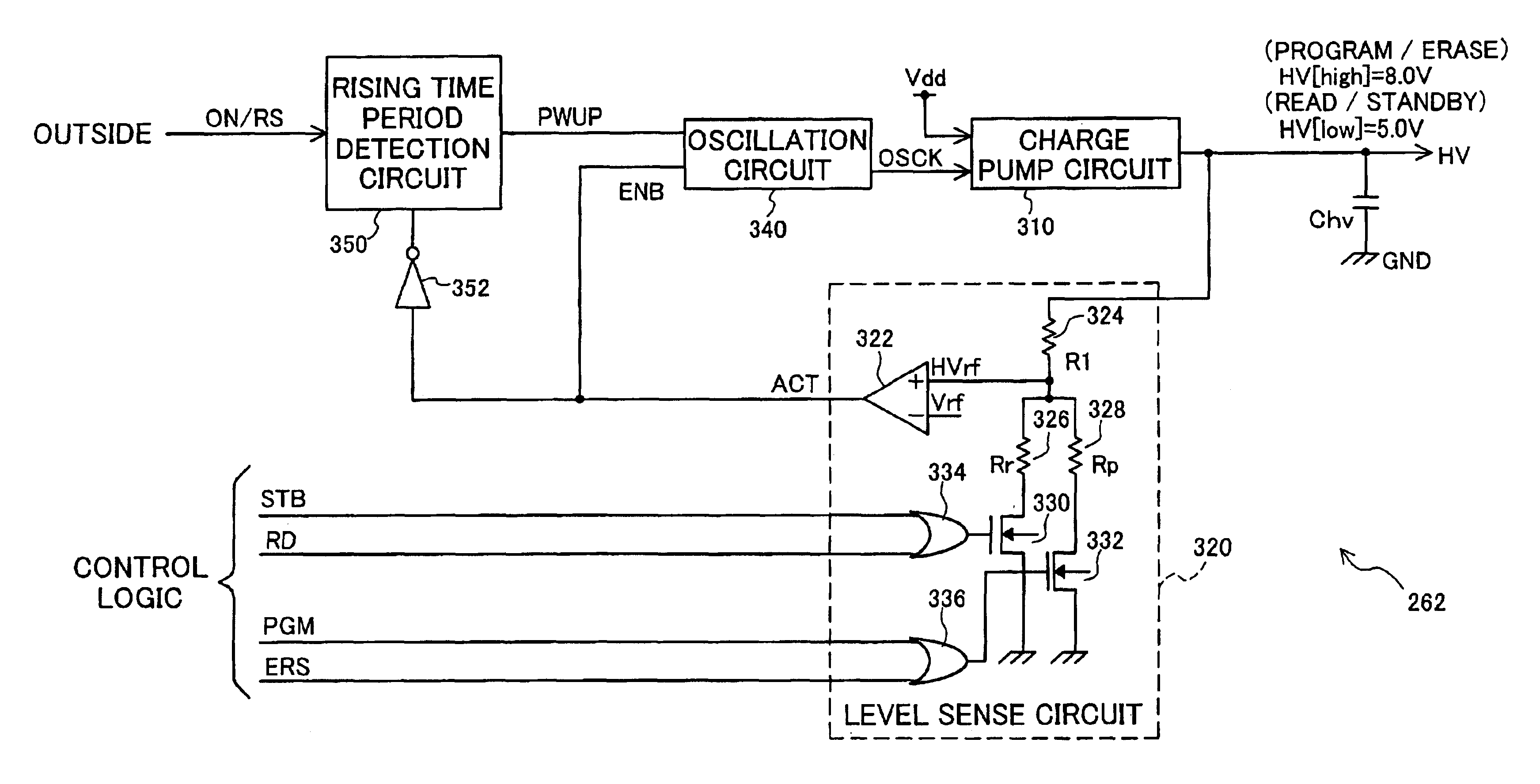
[0052]One mode of carrying out the present invention is discussed below as a preferred embodiment in the following sequence:[0053]A. Construction and Operations of Non-volatile Semiconductor Memory Device[0054]B. Structure and Operations of Memory Cells[0055]C. Structure and Operations of Voltage Generation Circuit[0056]D. Structure and Operations of Booster Circuit[0057]D-1. Operations at Power Supply ON time or at Reset Time[0058]D-2. Operations in Ordinary State[0059]D-3. Effects of Embodiment[0060]E. Modifications

A. Construction and Operations of Non-volatile Semiconductor Memory Device

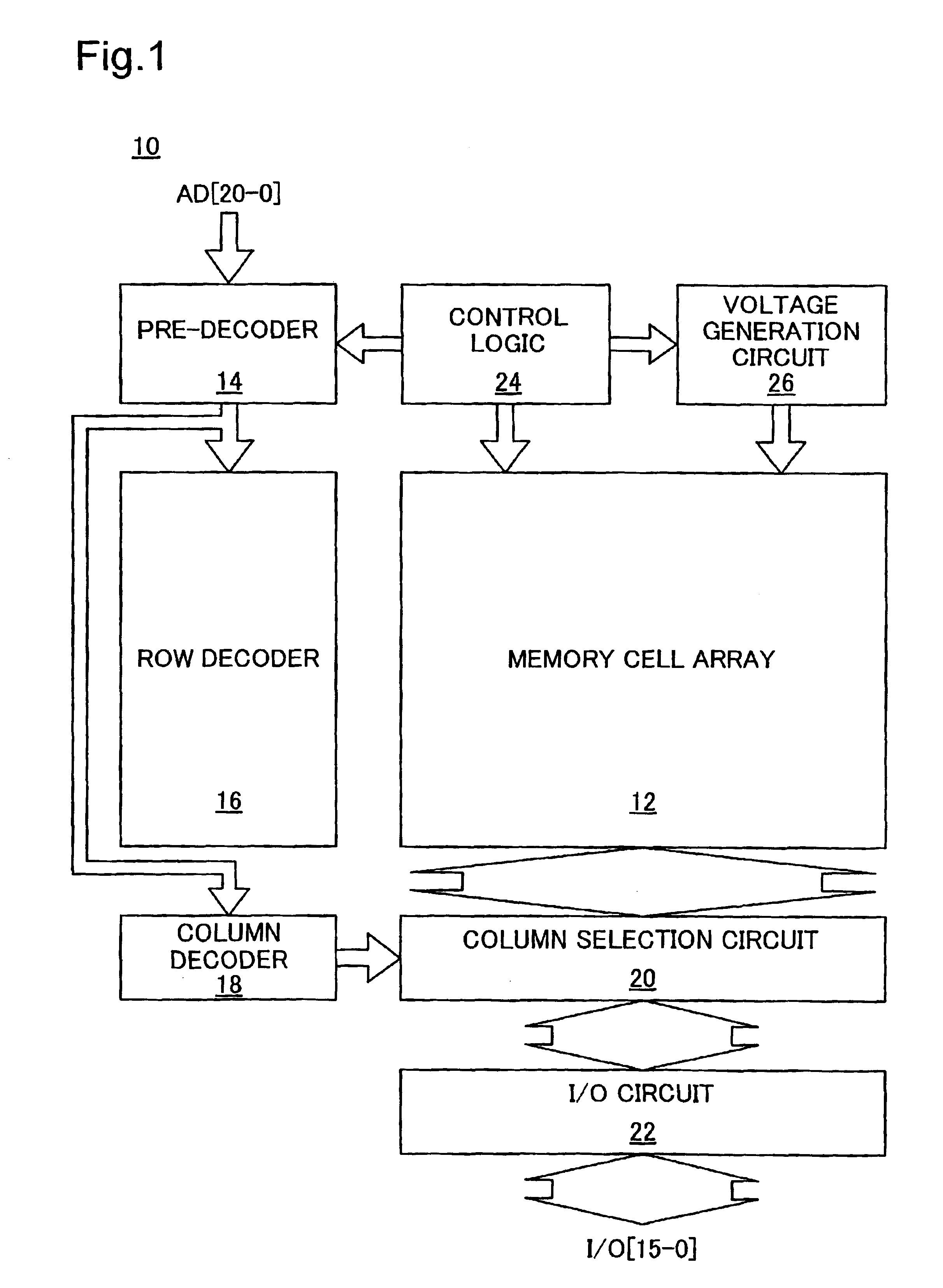
[0061]FIG. 1 is a block diagram schematically illustrating the general construction of a typical non-volatile semiconductor memory device 10. The non-volatile semiconductor memory device 10 mainly includes a memory cell array 12, a pre-decoder 14, a row decoder 16, a column decoder 18, a column selection circuit 20, an I / O circuit 22, a control logic 24, and a voltage generation circuit 26. The no...


PUM


Abstract

A detection circuit detects a rising time period between a power supply ON time or a reset time and a time when a boosted voltage reaches a standby voltage, and outputs a detection signal representing a result of the detection. An oscillation circuit generates an outputs a clock signal having a constant frequency which is lower than a frequency in an ordinary state, while the detection signal is at a high level. A charge pump circuit boosts a power source voltage in response to the input clock signal of the constant frequency and causes the boosted voltage to gently rise from the power source voltage, thereby effectively interfering with an increase in reference voltage accompanied by the increase in boosted voltage.

Description

BACKGROUND OF THE INVENTION[0001]1. Field of the Invention[0002]The present invention relates to a voltage generation circuit for a non-volatile semiconductor memory device. More specifically the invention pertains to a booster circuit that generates a boosted voltage from a power source voltage according to an operation mode.[0003]2. Description of the Related Art[0004]A semiconductor memory device has a memory cell array, in which multiple memory cells are arranged in a matrix. Data reading, programming or writing, and erasing operations with regard to each memory cell are generally carried out by specifying an address in a row direction and a column direction of the memory cell array.[0005]Regulation of a voltage applied to a signal line in the row direction and to a signal line in the column direction connected to each memory cell enables an access to the memory cell, in order to carry out a predetermined operation out of the data reading, programming, and erasing operations. Fo...

Claims


Application Information

Patent Timeline
IPC IPC(8): G11C16/04G11C16/06H01L21/70H01L21/822H01L31/0264H01L31/0328H01L27/04G11C5/14G11C8/08G11C16/30H01L27/115
CPCG11C5/145G11C16/30G11C8/08H01L27/115H10B69/00
Inventor NATORI, KANJI
Owner SEIKO EPSON CORP
Why Eureka
Try Eureka