Polymer optical waveguide and process for producing the same

a polymer optical waveguide and polymer technology, applied in the field of optical waveguides, can solve the problems of reducing the refractive index the precision of the obtained core diameter, and the insufficient difference between so as to achieve the effect of the cladding layer, and reducing the loss of the cor

Inactive Publication Date: 2005-05-31
FUJIFILM BUSINESS INNOVATION CORP
View PDF8 Cites 23 Cited by
  • Summary
  • Abstract
  • Description
  • Claims
  • Application Information

AI Technical Summary

Benefits of technology

[0014]That is, an objective of the invention is to provide simple and cost-effective process for producing a polymer optical waveguide having minimum waveguiding loss.
[0015]The above objectives are attained by the following invention. Specifically, the invention relates to a process for producing a polymer optical waveguide having minimum waveguiding loss and insertion loss by maintaining a highly precise core shape by employing capillary phenomenon proposed by the present inventors and, in particular, a method of reducing operating steps has been found.

Problems solved by technology

Problems to be solved still remain, however, in the above respective processes, as follows: The selective polymerization process (1) is problematic in lamination of the films, the processes (2) and (3) are costly since a photolithographic technique is adopted, the process (4) has a problem in precision of an obtained core diameter and the process (5) has a problem of providing no sufficient difference in refractive index between the core and cladding layers.
While processes excellent in performance and practical in use are currently limited to the processes (2) and (3), each has a cost problem to be solved.
As a result a problem arises in that light is leaked out through the thin layer.
However, in this process, unless a planar plate is joined using a clamp, other areas are undesirably immersed in monomer solution as well as the core part, hence a precise waveguide structure cannot be formed, being a troublesome process.
In addition, this process also has a defect that, when a monomer solution is polymerized to obtain a polymer (solidification), volumetric change occurs, which changes the shape of a core.
In addition, the process also has a defect that a polymer obtained by polymerizing a monomer solution and capillaries are partially adhered at removal of capillaries and, therefore, a core shape is destructed.
Even if a process described in the U.S. patent is applied to the producing of a polymer optical waveguide, it takes a long time to form a core portion, disabling application to mass production because of a small area of the core portion of an optical waveguide.
Furthermore, in the course of polymerization of a monomer solution to form a polymer, a change in volume occurs and a shape of the core is deformed, leading to a fault of a large transmission loss (waveguiding loss).

Method used


Image

  • Polymer optical waveguide and process for producing the same
  • Polymer optical waveguide and process for producing the same
  • Polymer optical waveguide and process for producing the same

Examples


example 1

[0118]After a thick resist (SU-8: manufactured by MicroChem Corp.) was coated on the surface of a Si substrate (diameter 6 inch) by a spin coating method, the substrate having the resist thereon was pre-baked at 80° C., irradiated with the light through a photomask, and developed to form a convex portion. Then, this was post-baked at 120° C., to prepare a master template for forming a core part of an optical waveguide having a branched concave portion. This optical waveguide is branched at 1:4 and, as shown in FIG. 3, has such a shape that a start point and an end point of a waveguide are aligned on the same straight line. A sectional-shape of a branched end is a regular square of 50 μm square, a length of a curved line part before and after branching is about 7.5 mm and they are arrayed at an interval of 250 μm at the end. In addition, a maximum width of a mixing part was 200 μm, lengths thereof were, in order from a shorter core part after branching, 19.75 mm, 20.00 mm, 20.25 mm a...

example 2

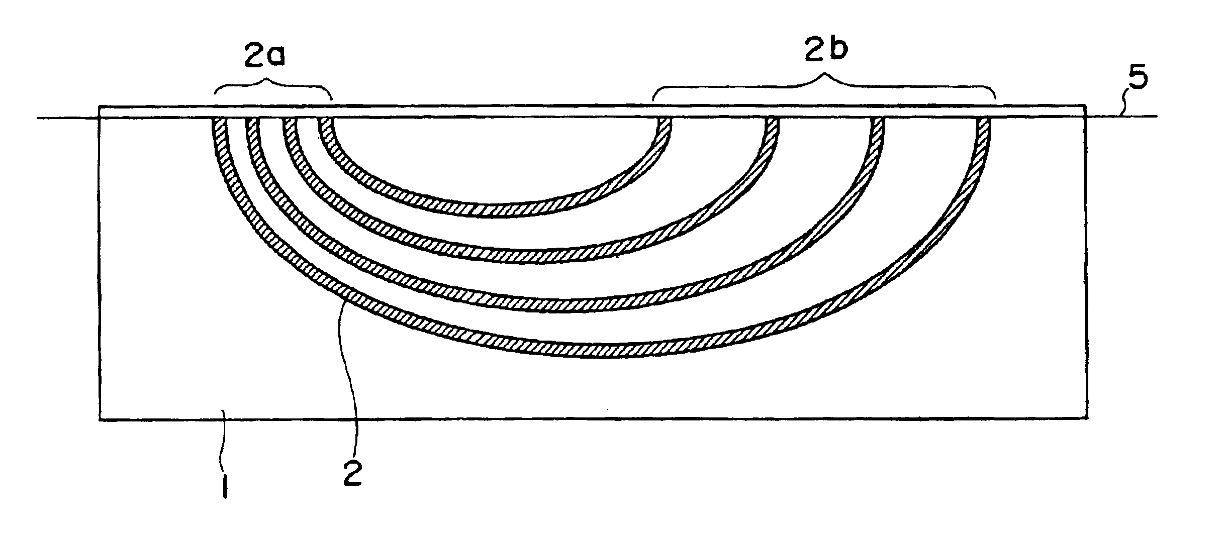
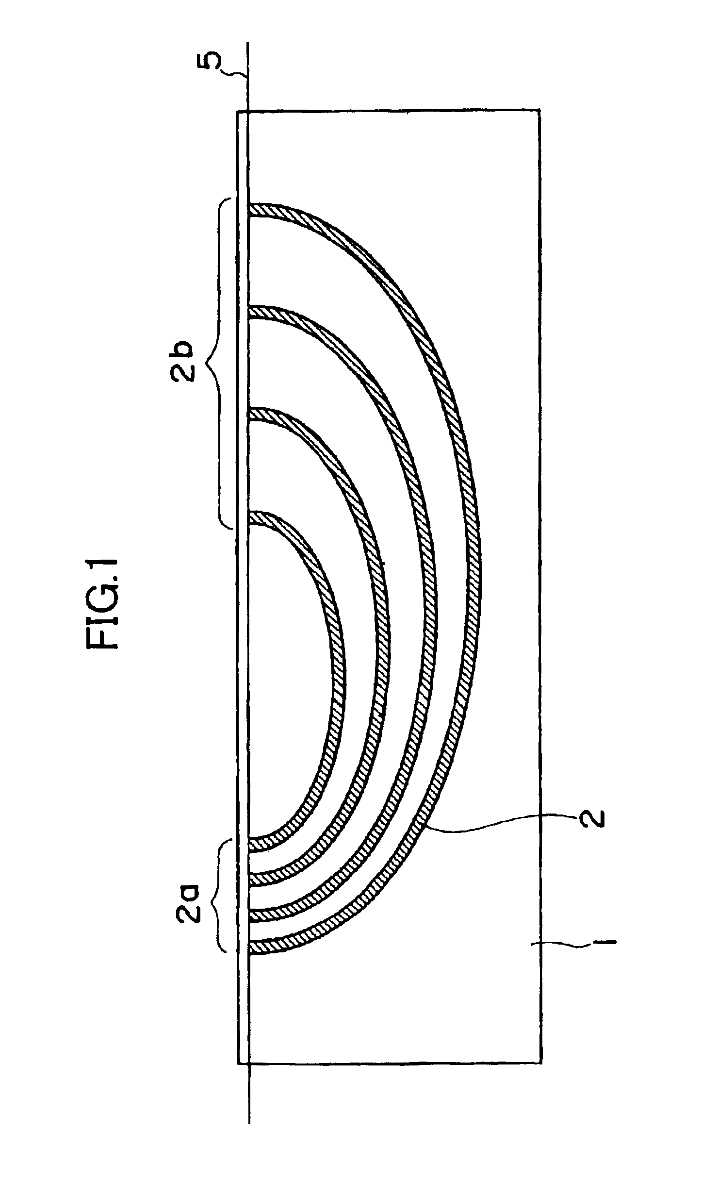
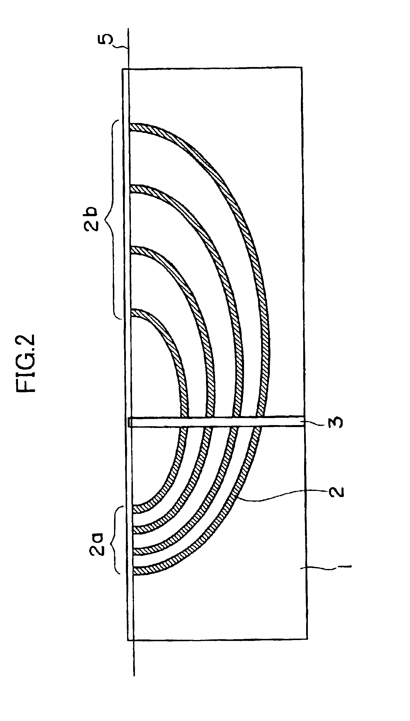
[0125]According to the same manner as that of Example 1, a master template for forming a core which has a cross-section of the regular square of 50 μm square was prepared. This core part structure has non-branched four waveguides and, as shown in FIG. 2, has a shape that a start point and an end point of a waveguide are aligned on the same straight line. A length of a waveguide is about 100 mm, and waveguides are arranged at a pitch of 250 μm.

[0126]A SUS plate having a thickness of 50 μm, on which a releasing agent was coated, was fixed at a position dividing a convex portion into approximately two parts in a longitudinal direction so as to cross the convex portion corresponding to the above 4 core parts. The plate was fixed not to be inclined. A releasing agent was coated on the whole and, thereafter, the PDMS resin used in Example 1 was poured. The resin was solidified by heating at 120° C. for 30 minutes, and removed to prepare a mold of a thickness of 3 mm having a concave porti...

example 3

[0133]A flexible polymer optical waveguide was prepared according to the same manner as that of Example 2 except that a resin inlet was not provided on an upper portion of a mold as in FIG. 1 and a core part was formed by utilizing a part corresponding to a start point of a waveguide as a resin inlet and a part corresponding to an end point as a resin outlet.

[0134]Upon this, a time for filling the ultraviolet ray-curable resin into the whole area of a concave portion of a mold was 30 minutes. In addition, the waveguiding loss of a polymer optical waveguide was 0.35 to 0.38 dB / cm.


PUM

PropertyMeasurementUnit
refractive indexaaaaaaaaaa
surface energyaaaaaaaaaa
RMS) roughnessaaaaaaaaaa

Abstract

A process for producing at least one polymer optical waveguide wherein each of at least one polymer optical waveguide has at least one start point and at least one end point uniformly aligned along a same single straight line. The process includes preparing a mold having at least one concave portion for forming at least one core; bringing a cladding substrate into close contact with the mold disposing the at least one concave portion towards the cladding substrate; filling the at least one concave portion of the mold with a core-forming curable resin; curing the core-forming curable resin in the at least one concave portion to form at least one core; and cutting a cladding substrate possessing at least one core part and a cladding layer thereon along the same single straight line.

Description

BACKGROUND OF THE INVENTION[0001]1. Field of the Invention[0002]The present invention relates to an optical waveguide, in particular, a flexible polymer optical waveguide, and also relates to a process for producing the polymer optical waveguide at low cost.[0003]2. Description of the Related Art[0004]Various kinds of processes for producing a polymer optical waveguide have been proposed, including: (1) a process in which films are impregnated with a monomer, a core portion is selectively exposed to light to alter a refractive index and then the films are stuck together (a selective polymerization process), (2) a process in which a core layer and a cladding layer are formed by coating, followed by application of reactive ion etching to form a clad portion (RIE method), (3) a process in which an ultraviolet ray-curable resin as a polymer material added with a photosensitive material thereto is exposed and developed using a photolithographic technique (a direct exposure method), (4) a...

Claims


Application Information

Patent Timeline
Patent Type & Authority Patents(United States)
IPC IPC(8): B29C39/02B29D11/00G02B6/13G02B6/125G02B6/122G02B6/138B29C33/00B29C39/26B29C69/00G02B6/12C08F2/46
CPCB29C39/02G02B6/122G02B6/1221G02B6/125G02B6/138B29D11/00663B29C33/0061B29C39/26B29C47/003B29C47/0066B29C69/001G02B2006/121B29K2995/0072B29C48/12B29C48/0022
Inventor SHIMIZU, KEISHIOHTSU, SHIGEMIYATSUDA, KAZUTOSHIAKUTSU, EIICHI
Owner FUJIFILM BUSINESS INNOVATION CORP
Why Eureka
Try Eureka