Low-temperature post-dopant activation process

a low-temperature, dopant activation technology, applied in the direction of semiconductor devices, material nanotechnology, electrical devices, etc., can solve the problems of deactivation of dopants in the source/drain region, and achieve the effect of reducing dopant deactivation and reducing dopant deactivation

Inactive Publication Date: 2005-06-07
ADVANCED MICRO DEVICES INC
View PDF22 Cites 7 Cited by
  • Summary
  • Abstract
  • Description
  • Claims
  • Application Information

AI Technical Summary

Benefits of technology

[0011]This and other needs are met by embodiments of the present invention which provide a method of manufacturing a semiconductor device that reduces dopant deactivation. The method comprises forming a gate electrode over a substrate and forming a gate oxide between the gate electrode and the substrate; forming source/drain extensions in the substrate; f

Problems solved by technology

A problem that exists with this process is that subsequent high-temperature pro

Method used


Image

  • Low-temperature post-dopant activation process
  • Low-temperature post-dopant activation process
  • Low-temperature post-dopant activation process

Examples


Embodiment Construction

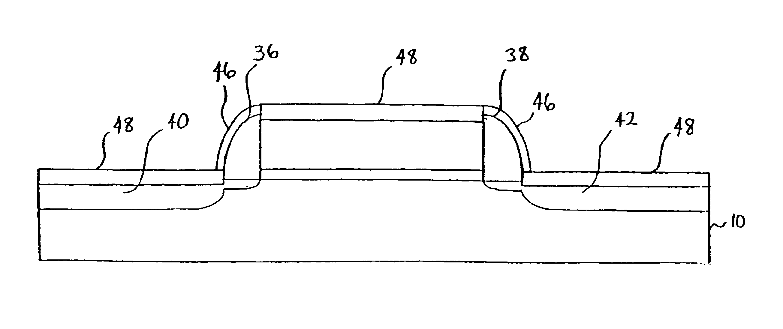
[0016]The present invention addresses and solves the problem of dopant deactivation as a result of high-temperature post-dopant activation processes, such as rapid thermal annealing. This is achieved, in part, by activating source / drain regions using laser thermal annealing, which is followed by a low-temperature salicide formation process. In particular, nickel silicide is formed over the activated source / drain region by applying a nickel layer over the source / drain region followed by a low-temperature furnace anneal. The temperature is sufficiently high to produce nickel silicide but sufficiently low to minimize dopant deactivation within the source / drain regions.

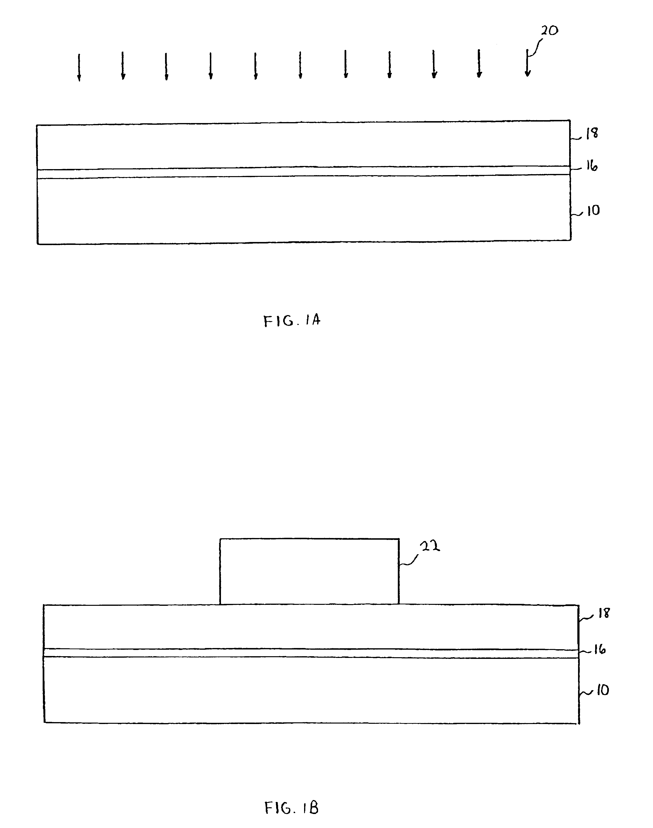
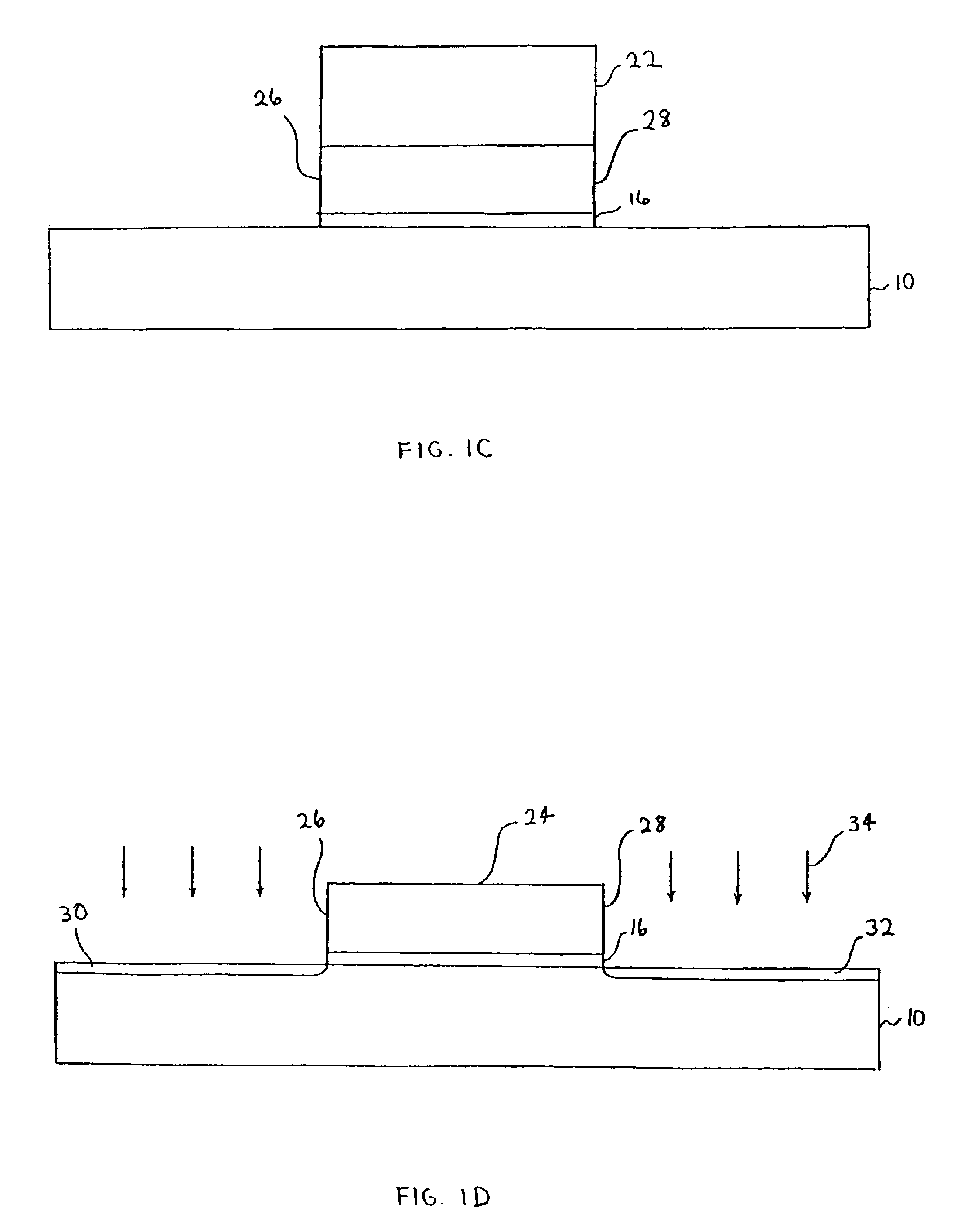
[0017]An embodiment of the present invention is illustrated in FIGS. 1A-1I. A silicon substrate is provided and can be formed from any material suitable for integrated circuit manufacture. However, in one aspect, the substrate is formed from single-crystal silicon, with a crystallographic orientation and which has been s...


PUM


Abstract

A method of manufacturing a MOSFET semiconductor device comprises forming a gate electrode over a substrate and a gate oxide between the gate electrode and the substrate; forming source/drain extensions in the substrate; forming first and second sidewall spacers; implanting dopants within the substrate to form source/drain regions in the substrate adjacent to the sidewalls spacers; laser thermal annealing to activate the source/drain regions; depositing a layer of nickel over the source/drain regions; and annealing to form a nickel silicide layer disposed on the source/drain regions. The source/drain extensions and sidewall spacers are adjacent to the gate electrode. The source/drain extensions can have a depth of about 50 to 300 angstroms, and the source/drain regions can have a depth of about 400 to 1000 angstroms. The annealing is at temperatures from about 350 to 500° C.

Description

FIELD OF THE INVENTION[0001]The present invention relates to the manufacturing of semiconductor devices, and more particularly, to post-laser anneal processes that prevent dopant deactivation.BACKGROUND OF THE INVENTION[0002]Over the last few decades, the semiconductor industry has undergone a revolution by the use of semiconductor technology to fabricate small, highly integrated electronic devices, and the most common semiconductor technology presently used is silicon-based. A large variety of semiconductor devices have been manufactured having various applications in numerous disciplines. One silicon-based semiconductor device is a metal-oxide-semiconductor (MOS) transistor. The MOS transistor is one of the basic building blocks of most modem electronic circuits. Importantly, these electronic circuits realize improved performance and lower costs, as the performance of the MOS transistor is increased and as manufacturing costs are reduced.[0003]A typical MOS semiconductor device ge...

Claims


Application Information

Patent Timeline
IPC IPC(8): H01L21/336H01L21/02H01L21/268H01L21/28H01L21/20H01L21/265H01L29/417H01L29/78
CPCH01L29/665H01L21/268B82Y30/00
Inventor YU, BINOGLE, ROBERT B.PATON, ERIC N.TABERY, CYRUS E.XIANG, QI
Owner ADVANCED MICRO DEVICES INC
Why Eureka
Try Eureka