Combined conformal/non-conformal seed layers for metallic interconnects

a technology of conformal/non-conformal seed layers and metallic interconnects, which is applied in the direction of basic electric elements, coatings, and heads using thin films, etc. it can solve the problems of low electroplating rate inside, poor or incomplete filling (voids) of high ar openings, and reducing growth inhibition inside the openings from the level achieved effect of high aspect ratio

Inactive Publication Date: 2005-06-07
COHEN URI DR
View PDF52 Cites 84 Cited by
  • Summary
  • Abstract
  • Description
  • Claims
  • Application Information

AI Technical Summary

Benefits of technology

[0014]Embodiments of the present invention advantageously satisfy the above-identified need in the art and provide a method and apparatus to produce seed layers used to produce void-free copper or silver electrochemical filling of small openings having high aspect ratios.

Problems solved by technology

Further, the higher the AR of the openings, the slower the electroplating rate is inside.
This results in poor or incomplete filling (voids) of high AR openings, when compared with results achieved with low AR openings.
Further, growth inhibition inside the openings is decreased from that achieved outside the openings due to slow replenishment of the additives inside the openings as compared with replenishment of the additives on the field.
Any voltage drop (and resulting non-uniformity therefrom) becomes more severe as the resistance of the seed layer increases due to high resistivity and / or insufficient thickness.
On the other hand, the typical thickness of about 300 Å to about 1,000 Å (on the field), deposited by the CVD techniques, may not be sufficient.
However, neither of these techniques satisfies all of the above-identified requirements.
The non-conformal PVD techniques, while providing adequate thickness on the field, fail to provide continuous and complete step coverage inside very narrow openings with large AR.
They also result in substantial overhangs at the top corners of the openings.
As a result, typical conformal CVD or electroless seed layers are too thin on the field and too thick inside the very narrow openings.

Method used


Image

  • Combined conformal/non-conformal seed layers for metallic interconnects
  • Combined conformal/non-conformal seed layers for metallic interconnects
  • Combined conformal/non-conformal seed layers for metallic interconnects

Examples


example 1

[0031]The following presents an example of a preferred embodiment of the inventive method for 0.18 μm wide vias or trenches. In accordance with the preferred embodiment, one deposits, by a CVD technique, a barrier layer comprised of about 200 Å of TaNX or WNX, then one deposits, by a CVD technique, a conformal seed layer comprised of about 300 Å of Cu, finally one deposits, by a PVD technique, a non-conformal seed layer comprised of about 900 Å of Cu (as measured on the field). This will result in a total combined (including the barrier) thickness of about 400 Å inside the openings: {Cu(PVD˜50 Å) / Cu(CVD˜250 ÅA) / TaNX(CVD˜100 Å)} and a total combined Cu seed layer and barrier layer thickness of about 1,400 Å on the field: {Cu(PVD˜900 Å) / Cu(CVD˜300 Å) / TaNX(CVD˜200 Å}. Advantageously, in accordance with the present invention, the inventive “two-step” seed layer deposition ensures a continuous seed layer having excellent step coverage, and a low-resistance electrical path on the field to...

example 2

[0043]FIGS. 5 and 6 show scanning electron microscope (“SEM”) photographs of a cross-section of a 0.10 μm wide trench having a Cu seed layer prepared in accordance with a preferred embodiment of the invention. In accordance with this embodiment, a pattern of trenches was formed in a SiO2 insulating layer. The trenches were about 0.10 μm wide and about 1.4 μm deep (thereby having an aspect ratio of about 14:1). Next, a barrier layer (WNX) was deposited using a CVD technique. Next, a relatively thin, conformal Cu seed layer was deposited using a CVD technique. The barrier layer and thin, conformal Cu seed layer is seen at 501 in FIG. 6. In accordance with this embodiment, the combined thickness of the barrier and the CVD Cu seed layer was about 500 Å on the field, and about 400-500 Å on the sidewalls and bottom of the trenches. Next, a non-conformal PVD Cu seed layer having a thickness of about 1,400 Å (on the field) was deposited by sputtering. In this embodiment, the non conformal P...

example 3

[0044]Similar to Example 2 above, trenches ˜0.10 μm wide and ˜1.4 μm deep (thereby having an aspect ratio of 14:1) were formed in a SiO2 insulating layer. Next, a barrier layer (WNX) was deposited using a CVD technique. Next, a relatively thin, conformal Cu seed layer was deposited using a CVD technique. The combined thickness of the barrier layer and the CVD Cu layer was ˜500 Å on the field, and ˜400-500 Å on the sidewalls and bottom of the trenches. Next, a non-conformal PVD Cu seed layer having a thickness of ˜500 Å (on the field) was deposited by sputtering. The end result was a combined thickness (including the barrier layer and the Cu seed layers) of only about 400-500 Å on the sidewalls and bottom of the trenches (with excellent continuity and uniformity), and about 1,000 Å on the field, without pinching-off the trenches.

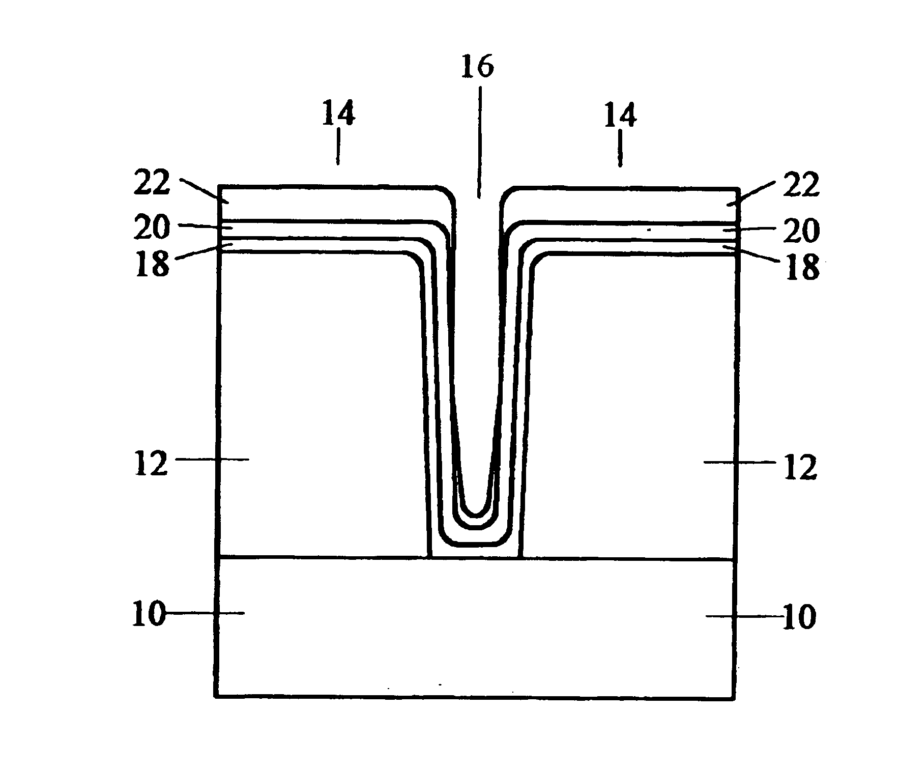
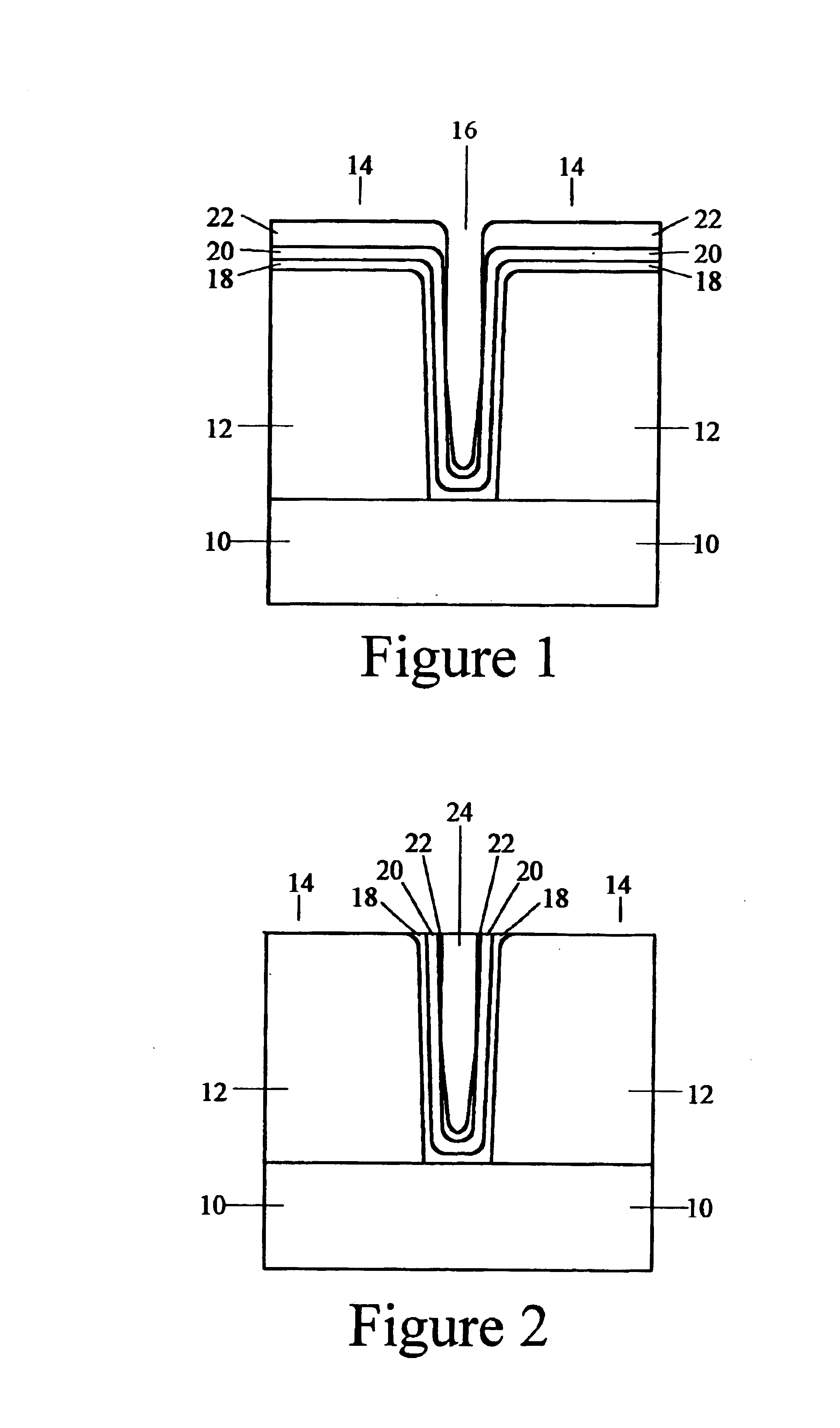
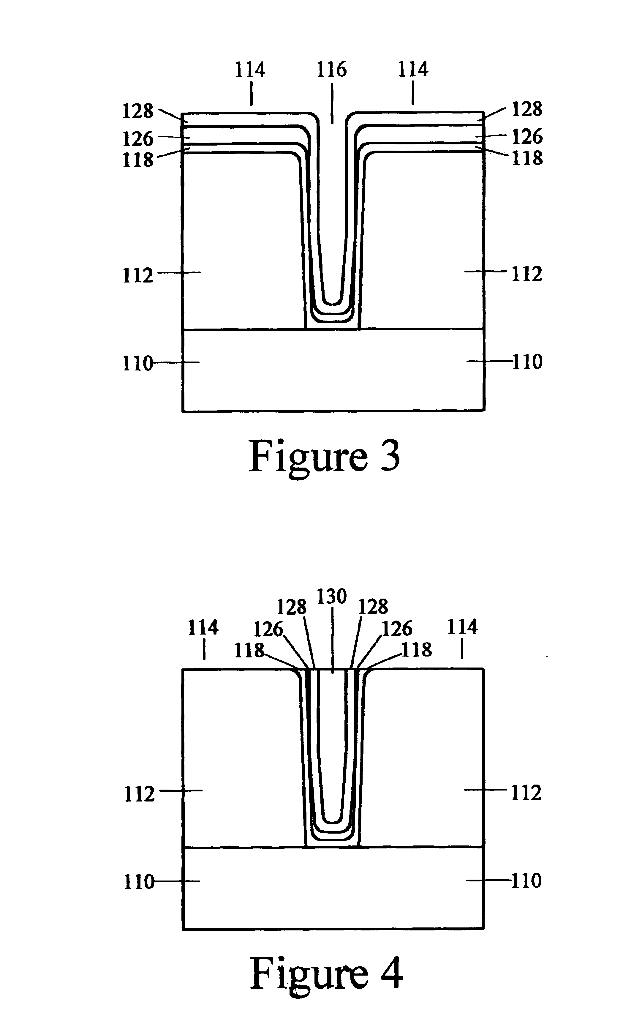
[0045]It should be understood that the scope of the present invention is not limited to the embodiments described above with respect to FIG. 1 and FIG. 3. Fo...


PUM

PropertyMeasurementUnit
tilt angleaaaaaaaaaa
thicknessaaaaaaaaaa
thicknessaaaaaaaaaa

Abstract

One embodiment of the present invention in a method for making copper interconnects, which method includes: (a) forming a patterned insulating layer on a substrate, the patterned insulating layer including at least one opening and a field surrounding the at least one opening; (b) depositing a barrier layer over the field and inside surfaces of the at least one opening; (c) depositing a non-conformal first copper seed layer over the barrier layer using physical vapor deposition, wherein the first seed layer is thicker than about 500 Å over the field; (d) depositing a conformal second copper seed layer over the first seed layer using chemical vapor deposition; and (e) electroplating a copper layer over the second seed layer.

Description

[0001]This is a continuation of a patent application Ser. No. 09 / 563,733, filed on May 3, 2000, now U.S. Pat. No. 6,610,151, which is a continuation-in-part of a patent application Ser. No. 09 / 410,898, filed on Oct. 2, 1999, now U.S. Pat. No. 6,136,707, issued on Oct. 24, 2000.TECHNICAL FIELD OF THE INVENTION[0002]The present invention pertains to the field of electroplating metals or alloys for filling high aspect ratio openings, such as trenches and vias, for semiconductor metallization interconnects, thin film heads, or micromachined Microelectromechanical Systems (MEMS) devices. In particular, embodiments of the present invention provide improved seed layers for electroplating copper or silver interconnects in semiconductor devices, and methods and apparatus for fabricating such improved seed layers. The improved seed layers facilitate reliable, void-free filling of small openings with high aspect ratios for so called “Damascene” and “Dual Damascene” copper and / or silver interco...

Claims


Application Information

Patent Timeline
Patent Type & Authority Patents(United States)
IPC IPC(8): H01L21/70H01L21/768C25D7/12G11B5/31H01L21/285H01L21/288H01L21/3205H01L23/52
CPCH01L21/76843H01L21/76873H01L2221/1089
Inventor COHEN, URI
Owner COHEN URI DR
Why Eureka
Try Eureka