Organic electroluminescent element, displaying apparatus, light emitting method, displaying method and transparent substrate

Inactive Publication Date: 2005-06-07
KONICA CORP
View PDF12 Cites 25 Cited by
  • Summary
  • Abstract
  • Description
  • Claims
  • Application Information

AI Technical Summary

Benefits of technology

[0014]The object of the invention is to provide an organic EL element having a high light emitting efficiency, a wide visible angle and that without a color change depending on the viewing angle, a light emission metho

Problems solved by technology

However, it is a problem that red light having a sufficient intensity is difficultly obtained through the color conversion member since the light emitted from the organic EL member is blue or blue-green.
Moreover, the light is largely lost when the light is conducted from the light emission member to the light conversion member since the light emitted from the light-emitting layer has no directivity and scatters in all directions.
Accordingly, the intensity of the light is made insufficient and the displayed image becomes too dark.
However, a problem that the wide visible angle cannot be obtained because of the directivity of the emitted light is occurred when the organic EL element having the micro optical resonator structure is applied for the displaying apparatus.
Furthermore, there is a problem on the colo

Method used


Image

  • Organic electroluminescent element, displaying apparatus, light emitting method, displaying method and transparent substrate
  • Organic electroluminescent element, displaying apparatus, light emitting method, displaying method and transparent substrate
  • Organic electroluminescent element, displaying apparatus, light emitting method, displaying method and transparent substrate

Examples


Example

Example 1-2

[0201]A transparent substrate using the transparent resin film as the constituting material and having the dielectric mirror structure was prepared in the same manner as in Example 1-1 except that the silicon oxide layers and the titanium oxide layers were each replaced by silicon oxonitride layers and titanium oxonitride layers, respectively. It was confirmed that thus prepared transparent substrate was considerably improved in the moisture proof ability. (Compared to Example 1-1)

Example

Example 2

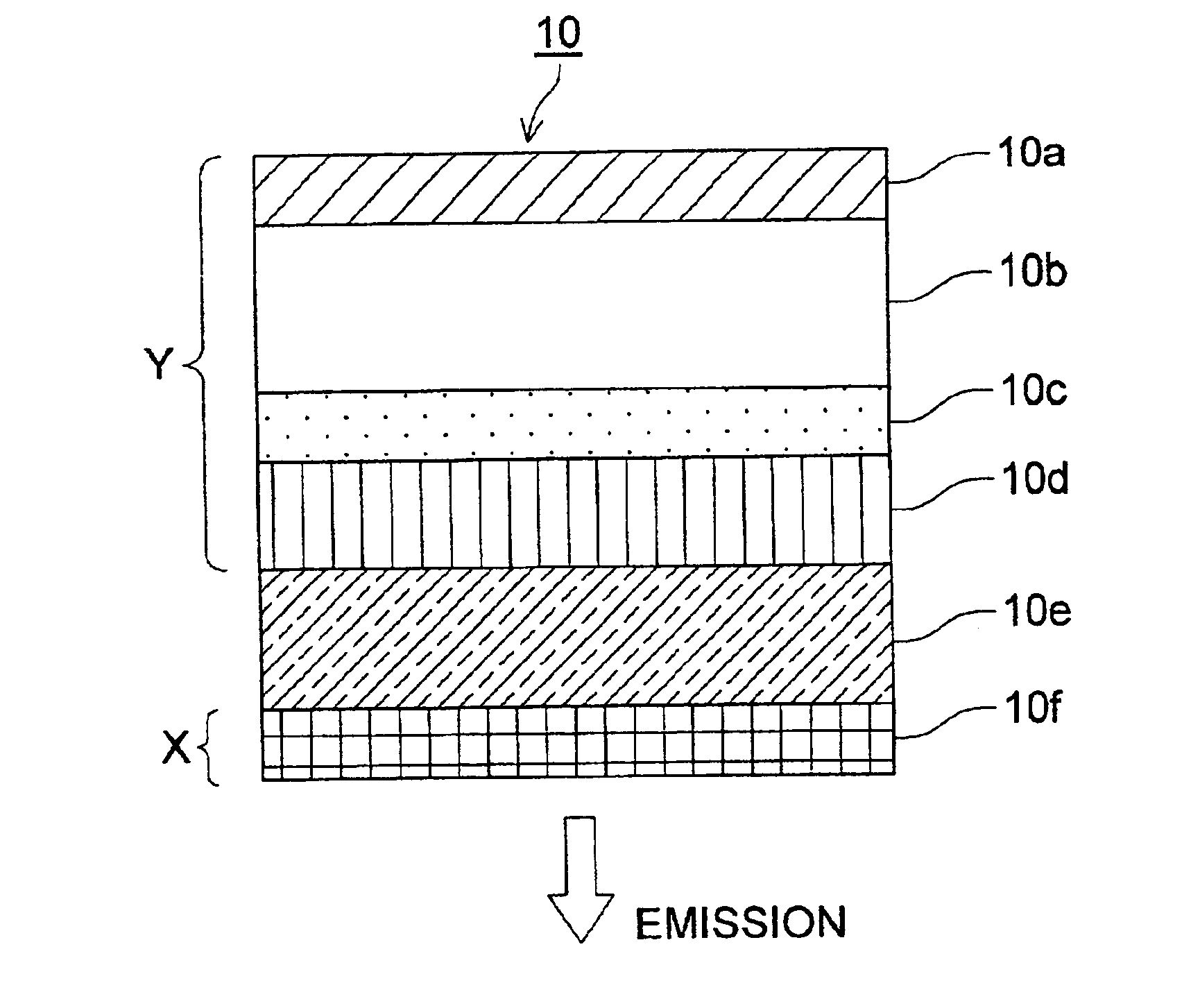
[0202]A transparent electrically-conductive layer, ITO, having a thickness of 50 nm was formed as an anode on the dielectric mirror of the transparent substrate prepared in Example 1-1 by the RF-magnetron spattering method. Thus prepared substrate was fixed in a vacuum deposition apparatus after sufficient washing by an organic solvent. An m-MTDATXA layer with a thickness of 20 nm as the hole transporting layer, a layer of DMPhen with a thickness of 20 nm as a light-emitting layer and a basocuproin (BC) layer with a thickness of 20 nm were deposited. Then the total thickness of the transparent electrically-conductive layer and the organic compound thin layers was 110 nm. DMPhen is the foregoing BP-13. The structures of m-MTDATXA and BC are shown below.

[0203]The optical length of the micro optical resonator in the thus obtained element was 1.5 times of the objective wavelength of 405 nm according to the foregoing Equation 1 based on the thickness and the refractive index of...

Example

Comparative example 1

[0218]A transparent substrate having the dielectric structure was prepared in the same manner as in Example 1 except that the thickness of the SiO2 layer and the TiO2 layer were each changed to 79 nm and 48 nm, respectively.

[0219]A transparent electrically-conductive layer ITO with a thickness of 50 nm was formed by the RF-magnetron spattering method on the thus obtained transparent substrate having the dielectric mirror. The substrate was sufficiently washed and fixed in the vacuum deposition apparatus. Then an m-MTDATA layer with a thickness of 40 nm as the hole transporting layer, a layer of DPVBi with a thickness of 25 nm as a light-emitting layer and an Alq3 layer with a thickness of 10 nm were deposited. Then the total thickness of the transparent electrically-conductive layer and the organic compound thin layers was become 125 nm.

[0220]The structures of m-MTDATA, DPVBi and Alq3 are shown below.

[0221]The optical length of the micro optical resonator in th...


PUM


Abstract

An organic electroluminescent element is disclosed. The organic electroluminescent element has a micro optical resonator structures, an organic electroluminescent member emitting light within the color region of bluish purple and a color conversion member emitting visible fluorescent by absorbing the light emitted from the organic light emitting member.

Description

FIELD OF THE INVENTION[0001]The present invention relates to an organic electroluminescent element, hereinafter simply referred to as an organic element, a displaying apparatus, a light emitting method, a displaying method and a transparent substrate.BACKGROUND OF THE INVENTION[0002]An inorganic electroluminescent element has been used as a flat type light source. An alternative high voltage is required to drive such the inorganic electroluminescent element.[0003]A recently developed organic EL element is an element has a structure in which an organic compound thin layer containing an organic fluorescent compound is arranged between a cathode and an anode. The EL element emits light, fluorescence or phosphorescence, when the excitons formed by recombination of electrons and holes injected into the thin layer are deactivated. To utilize the emitted light, at least one of the electrodes each arranged at both sides of the organic compound thin layer is usually a transparent electrode s...

Claims


Application Information

Patent Timeline
IPC IPC(8): H01L51/50H01L27/32H01L27/28H05B33/12H05B33/02H05B33/04H05B33/24
CPCH01L51/5265H01L51/5036H01L27/322H10K59/38H10K50/125H10K50/852
Inventor KITA, HIROSHIOSHIYAMA, TOMOHIRO
Owner KONICA CORP
Why Eureka
Try Eureka