Dielectric filler containing resin for use in formation of built-in capacitor layer of printed wiring board and double-sided copper clad laminate with dielectric layer formed using the same dielectric filler containing resin, and production method of double-sided copper clad laminate

a technology of dielectric filler and resin, which is applied in the direction of fixed capacitors, synthetic resin layered products, solid-state devices, etc., can solve the problems of copper layer destruction, inconvenience, and hardly possible to make the electrode area larger

Inactive Publication Date: 2005-06-14
MITSUI MINING & SMELTING CO LTD
View PDF7 Cites 23 Cited by
  • Summary
  • Abstract
  • Description
  • Claims
  • Application Information

AI Technical Summary

Benefits of technology

[0012]As a result of diligent study, the present inventors have thought out that the use of a dielectric filler containing resin and a dielectric filler powder, for use in formation of a built-in capacitor layer in a printed wiring board, makes it possible to form a dielectric layer provided with sufficient strength and dielectric constant even under omission of a skeletal material.

Problems solved by technology

However, as far as the surface area (A) described above in is concerned, it is hardly possible to make the area of the capacitor electrode larger in a certain constrained area of a printed wiring board because a printed wiring board is demanded to be lighter and more compact in conformity with the recent trend that electronic and electric appliances are being made lighter and more compact.
On the other hand, if the skeletal material is merely omitted while using a conventional dielectric layer constituting material, an inconvenience occurs that a copper layer is destructed in a portion of the dielectric layer where the copper foil is removed by etching, through the shower pressure of the etching solution that is used in etching for forming a capacitor electrode.
The migration phenomenon in a dielectric layer containing a skeletal material refers to a phenomenon that the copper component of the copper plating layer in the print wiring board and the metallic component constituting the dielectric filler diffuse to migrate electrophoretically along the interface between the skeletal material and the resin layer and thus causes inconvenience of short circuiting between neighboring circuits.

Method used


Image

  • Dielectric filler containing resin for use in formation of built-in capacitor layer of printed wiring board and double-sided copper clad laminate with dielectric layer formed using the same dielectric filler containing resin, and production method of double-sided copper clad laminate
  • Dielectric filler containing resin for use in formation of built-in capacitor layer of printed wiring board and double-sided copper clad laminate with dielectric layer formed using the same dielectric filler containing resin, and production method of double-sided copper clad laminate
  • Dielectric filler containing resin for use in formation of built-in capacitor layer of printed wiring board and double-sided copper clad laminate with dielectric layer formed using the same dielectric filler containing resin, and production method of double-sided copper clad laminate

Examples


example 1

[0058]In the present example, description will be made with reference to FIGS. 1 and 2. At the beginning, a binder resin solution was produced. In the production of the binder resin solution, the raw material used were 25 parts by weight of phenol novolac type epoxy resin, 25 parts by weight of a solvent soluble aromatic polyamide resin polymer, and BP3225-50P from Nippon Kayaku Co., Ltd. commercially available as a mixed varnish mixed with cyclopentanone as solvent. Additionally, a resin mixture having the blending ratios shown below was prepared by adding a novolac type phenolic resin, MEH-7500 from Meiwa Kasei Co., Ltd., as a curing agent and 2E4MZ from Shikoku Kasei Co., Ltd. as a curing accelerator to the mixed varnish.

[0059]

The composition of the binder resinPhenol novolac type epoxy resin 39 parts by weightAromatic polyamide resin polymer 39 parts by weightNovolac type phenolic resin 22 parts by weightCuring accelerator0.1 parts by weight

[0060]The resin mixture was adjusted t...

example 2

[0066]In the present example, description will be made with reference to FIGS. 3 and 4. A dielectric filler containing resin solution was produced by a method similar to that in Example 1. Accordingly, the description for the production method of the dielectric filler containing resin solution is omitted because the description becomes redundant.

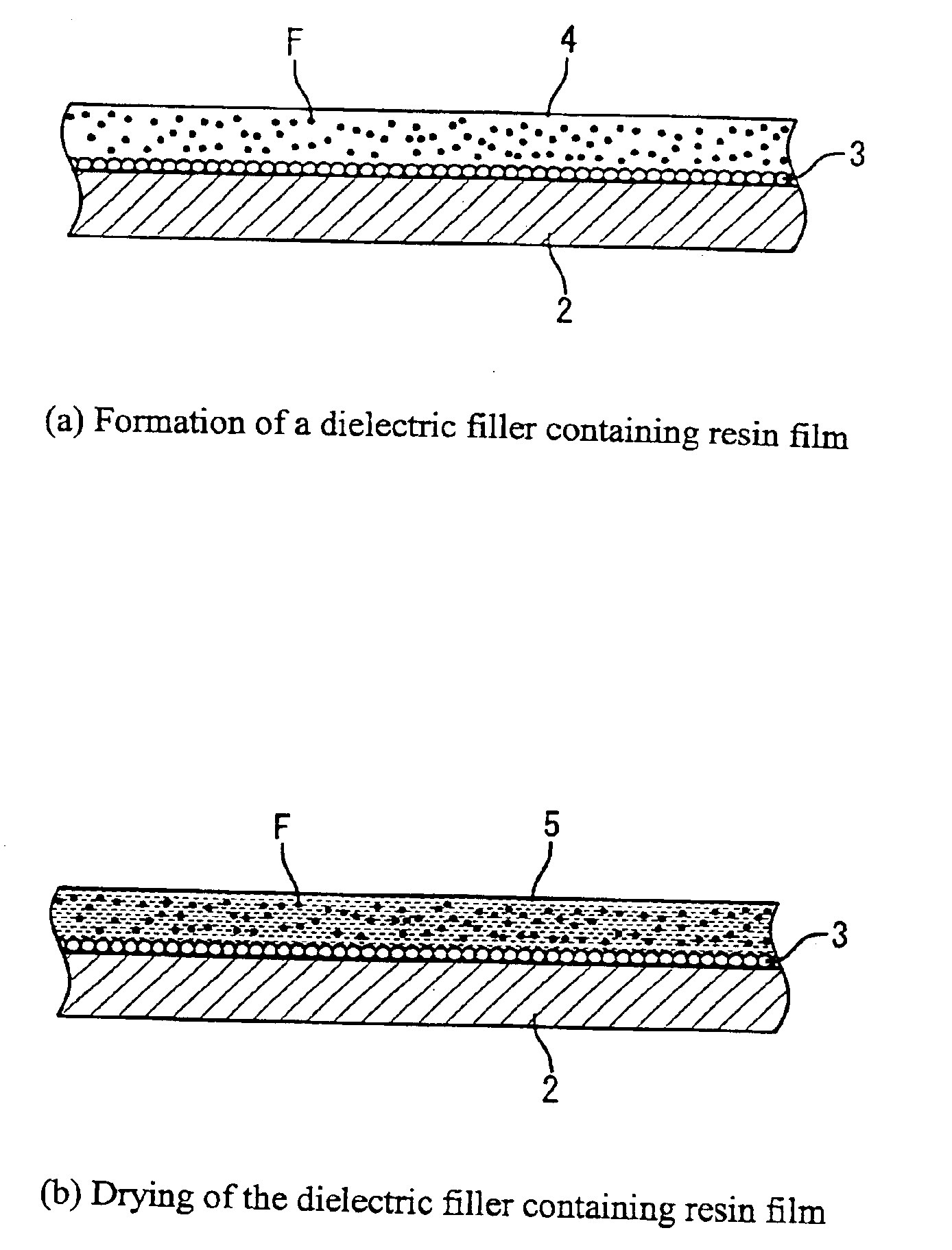
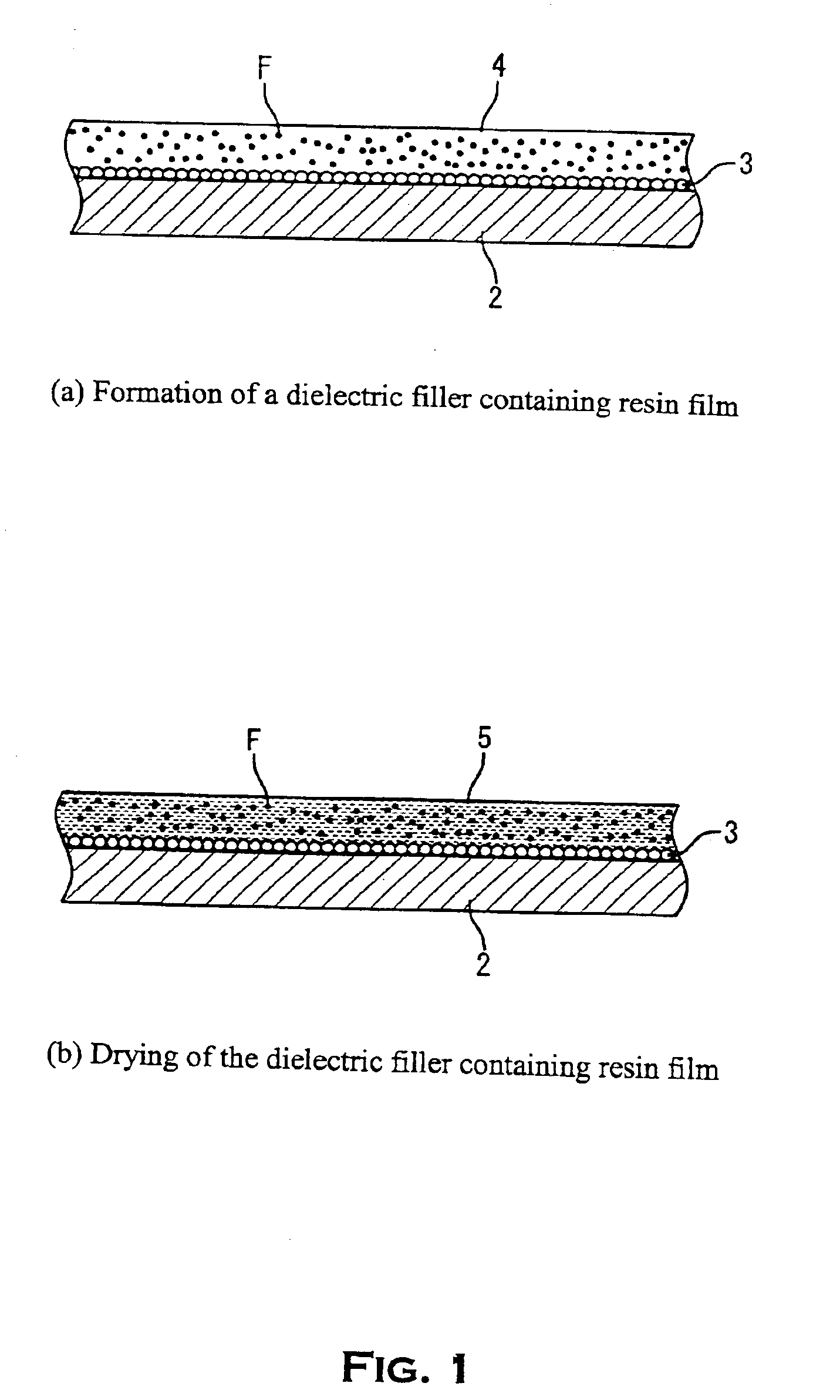
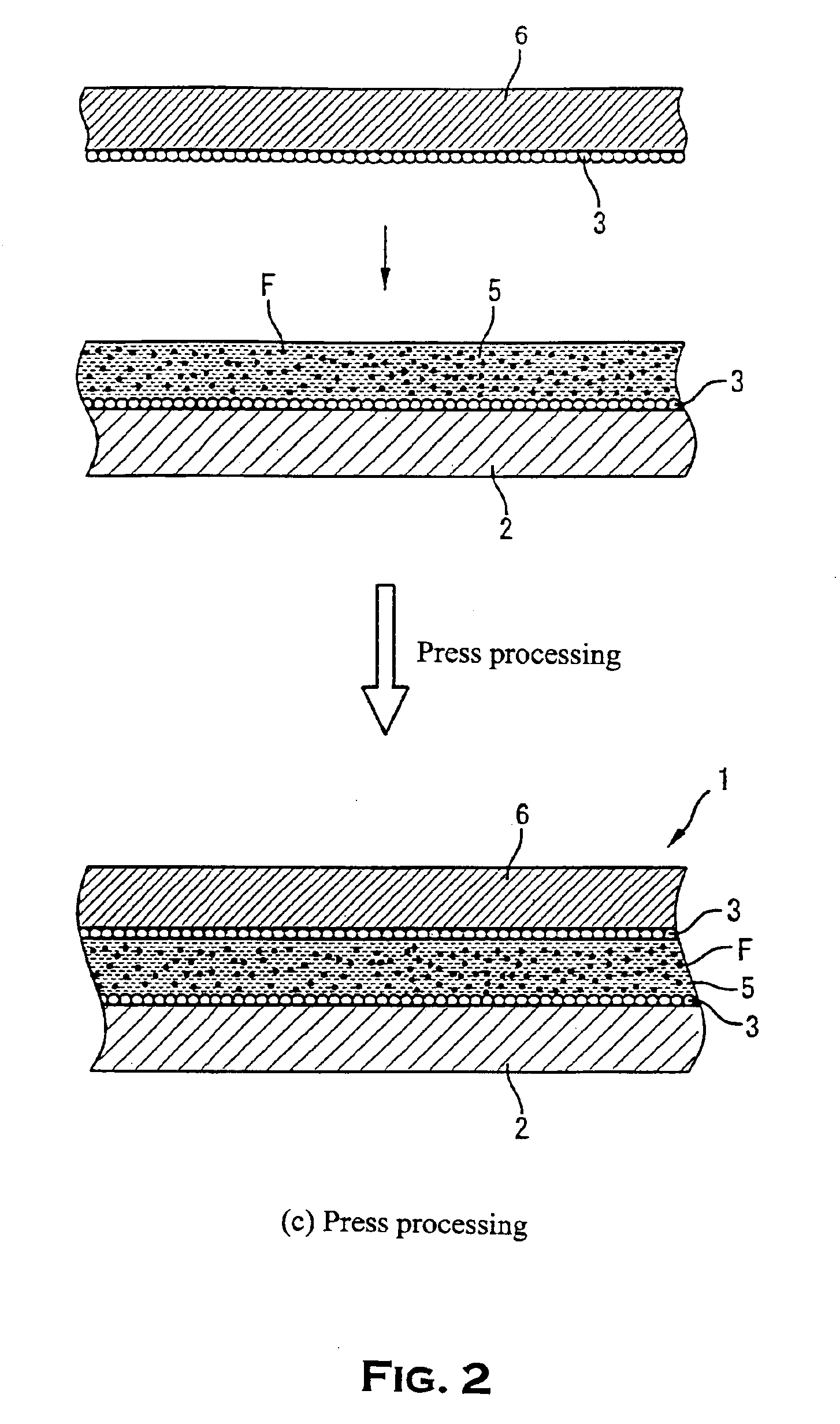
[0067]In the present example, the dielectric filler containing resin solution was applied, using an edge coater, as the process shown in FIG. 3(a), onto the nodularized surface of the first copper foil 2 so as to form a 5 μm thick dielectric filler containing resin film 4, air drying was conducted for 5 minutes, then a drying processing was conducted for 5 minutes in a heated atmosphere at 150° C., and thus an about 5 μm thick semicured-state dielectric layer 5a, shown in FIG. 3(b), was formed. Additionally, as FIG. 4(c) shows, the application was once again made so as to form a 5 μm thick dielectric filler containing resin film 4 on the fir...


PUM

PropertyMeasurementUnit
particle size D50aaaaaaaaaa
thicknessaaaaaaaaaa

Abstract

An object is to provide a dielectric layer of a double-sided copper clad laminate, for use in formation of a built-in capacitor layer, which can be formed in an optional thickness without using a skeletal material and is provided with a high strength. For the purpose of achieving the object, “a dielectric filler containing resin for use in formation of the built-in capacitor layer of a printed wiring board obtained by mixing a binder resin comprising 20 to 80 parts by weight of epoxy resin (inclusive of a curing agent), 20 to 80 parts by weight of a solvent soluble aromatic polyamide resin polymer, and a curing accelerator added in an appropriate amount according to need; and a dielectric filler which is a nearly spherical dielectric powder having perovskite structure which is 0.1 to 1.0 μm in the average particle size DIA, 0.2 to 2.0 μm in the weight cumulative particle size D50 based on the laser diffraction scattering particle size distribution measurement method, and 4.5 or less in the coagulation degree represented by D50/DIA where the weight cumulative particle size D50 and the average particle size DIA obtained by the image analysis”; and the like are used.

Description

CROSS REFERENCE TO RELATED APPLICATION[0001]This application is a 35 USC § 371 National Phase Entry Application from PCT / JP03 / 04172 filed Apr. 1, 2003, and designating the U.S.TECHNICAL FIELD[0002]The present invention relates to a dielectric filler containing resin for use in the formation of a built-in capacitor layer of a printed wiring board, a double-sided copper clad laminate in which a dielectric layer is formed by using the dielectric filler containing resin, and a production method of the double-sided copper clad laminate.BACKGROUND ART[0003]In these years, it has become general practice that a capacitor structure is formed by using a copper clad laminate in a printed wiring board, in particular, in the internal layer portion of a multilayer printed wiring board, in a manner similar to that in circuit shape formation, and the capacitor structure thus formed is utilized as a built-in capacitor. The formation of a capacitor structure in the internal layer portion of a multila...

Claims


Application Information

Patent Timeline
Patent Type & Authority Patents(United States)
IPC IPC(8): C08L63/00H05K1/16C08L77/00C08K7/00C08L77/10H05K3/38B32B15/08B32B27/18B32B27/34B32B27/38C08K7/16H01L23/12
CPCC08L63/00H05K1/162C08K7/00C08L77/00C08L77/10H05K3/384Y10T428/25H05K2201/0355H05K2201/09309H05K2203/1476H05K2201/0209Y10T428/24917C08L2666/20C08K3/22C08K3/10
Inventor MATSUSHIMA, TOSHIFUMIMIWA, HIDEAKIICHIRYU, AKIRAYAMAZAKI, KAZUHIROSATO, TETSUROKUWAKO, FUJIO
Owner MITSUI MINING & SMELTING CO LTD
Why Eureka
Try Eureka