Method using TEOS ramp-up during TEOS/ozone CVD for improved gap-fill

a technology of ozone and teos, which is applied in the direction of coatings, chemical vapor deposition coatings, semiconductor devices, etc., can solve the problems of high operating power consumption, more likely that the void will not be filled, and the topology of the pattern can interfere with or degrade subsequent wafer processing, etc., to achieve good gap-filling properties, increase the ratio of silicon-containing gas to oxidizing gas, and high throughput

Inactive Publication Date: 2005-06-14
APPLIED MATERIALS INC
View PDF17 Cites 33 Cited by
  • Summary
  • Abstract
  • Description
  • Claims
  • Application Information

AI Technical Summary

Benefits of technology

[0008]The present invention provides methods and apparatuses related to chemical vapor deposition of silicon oxide. In one embodiment, a single-step deposition process is used to efficiently form a silicon oxide layer exhibiting good gap-filling properties with high throughput. The silicon oxide layer is initially formed under conditions including a relatively low ratio of silicon-containing gas:oxidizing gas. As the CVD process step continues, the ratio of silicon-containing gas:oxidizing gas is increased. As a result of these changed processing conditions, silicon oxide of a highly conformal character is formed relatively slowly during initial stages of the deposition step, with less conformal oxide formed more rapidly during later stages, thereby allowing for high throughput.

Problems solved by technology

The topology of the pattern can interfere with or degrade subsequent wafer processing.
While the reduction in feature size has allowed higher device density, more chips per wafer, more complex circuits, lower operating power consumption and lower cost among other benefits, the smaller geometries have also given rise to new problems, or have resurrected problems that were once solved for larger geometries.
An example of the type of manufacturing challenge presented by sub-micron devices is the ability to completely fill a narrow trench in a void-free manner.
However, as the trench becomes narrower, it becomes more likely that the void will not be filled during the reflow process.
Moreover, several types of applications call for the deposition of undoped silicon oxide, which is difficult to reflow even at elevated temperature.
Voids resulting from pinching-off are undesirable as they can reduce the yield of good chips per wafer and the reliability of the devices.
However, such a two-step process may exhibit reduced throughput due to the extended time required in the first step, and also the time consumed in halting the process gas flow and changing the apparatus configuration between the first and second steps.

Method used


Image

  • Method using TEOS ramp-up during TEOS/ozone CVD for improved gap-fill
  • Method using TEOS ramp-up during TEOS/ozone CVD for improved gap-fill
  • Method using TEOS ramp-up during TEOS/ozone CVD for improved gap-fill

Examples


Embodiment Construction

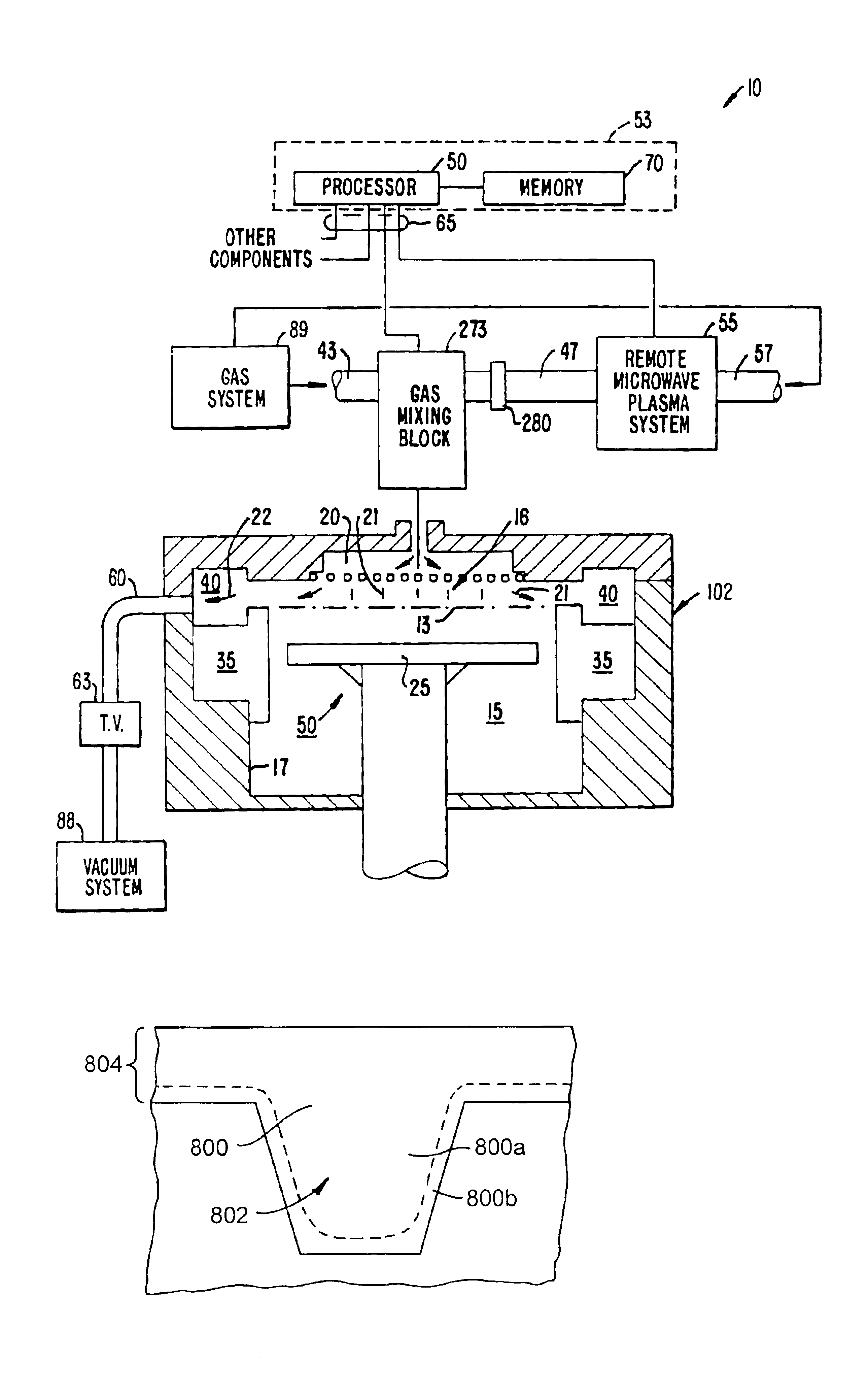
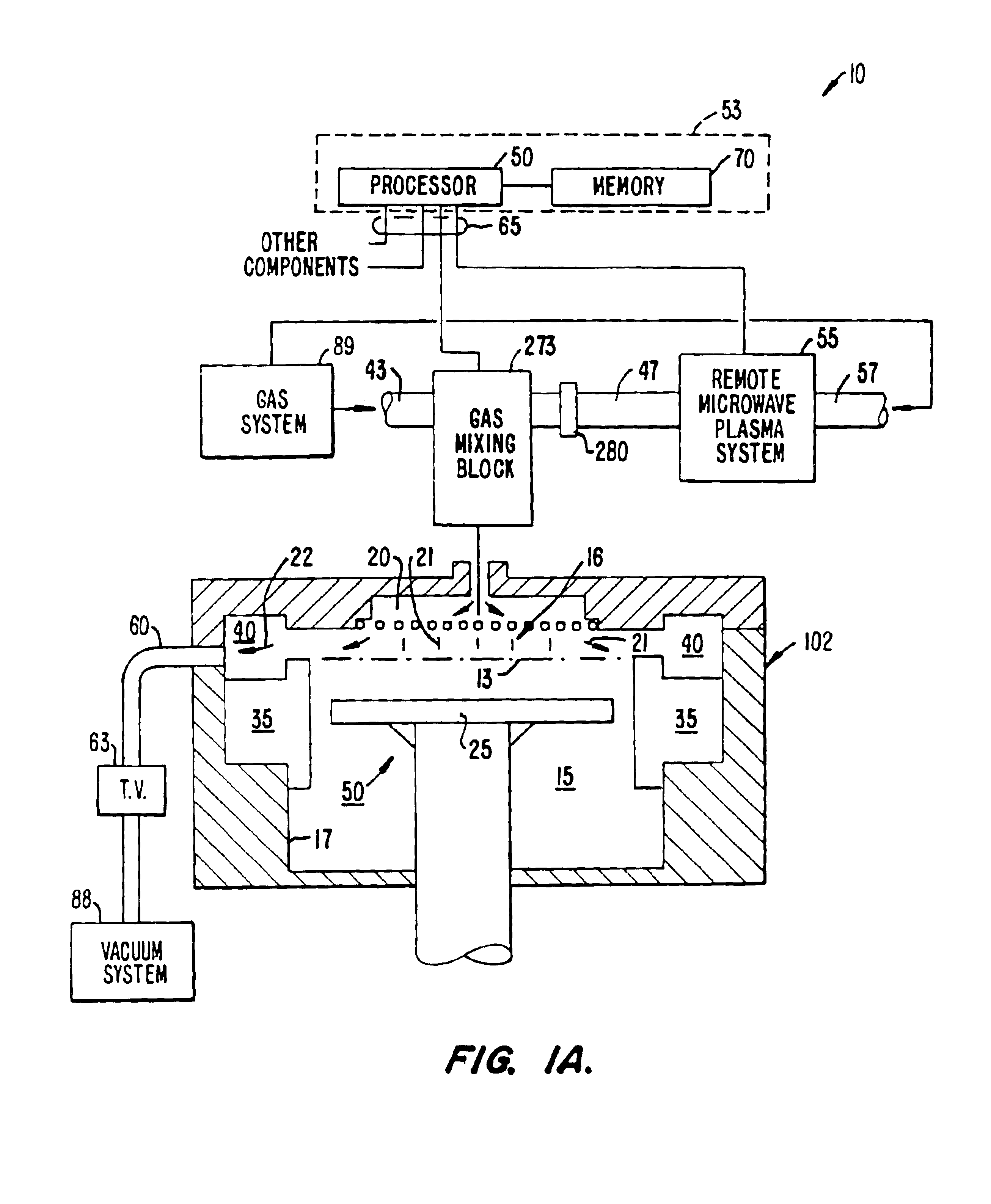
[0026]The present invention provides methods and apparatuses related to chemical vapor deposition of silicon oxide. In one embodiment, a single-step deposition process is used to efficiently form a silicon oxide layer exhibiting good gap-filling properties with high throughput. The silicon oxide layer is initially formed under conditions including a relatively low ratio of silicon-containing gas:oxidizing gas. As the CVD process step continues, the ratio of silicon-containing gas:ozone is increased. As a result of these changed processing conditions, silicon oxide of a highly conformal character is formed relatively slowly during initial stages of the deposition process step, with less conformal oxide formed more rapidly during later stages, thereby allowing for high throughput.

[0027]For purposes of this application, the term “deposition step” refers to a period of continuous flow of a silicon-containing gas to a processing chamber. The term “stage” refers to a portion of a depositi...


PUM

PropertyMeasurementUnit
temperaturesaaaaaaaaaa
flow rateaaaaaaaaaa
timeaaaaaaaaaa

Abstract

Embodiments of the present invention provide methods, apparatuses, and devices related to chemical vapor deposition of silicon oxide. In one embodiment, a single-step deposition process is used to efficiently form a silicon oxide layer exhibiting high conformality and favorable gap-filling properties. During a pre-deposition gas flow stabilization phase and an initial deposition stage, a relatively low ratio of silicon-containing gas:oxidant deposition gas is flowed, resulting in formation of highly conformal silicon oxide at relatively slow rates. Over the course of the deposition process step, the ratio of silicon-containing gas:oxidant gas is increased, resulting in formation of less-conformal oxide material at relatively rapid rates during later stages of the deposition process step.

Description

BACKGROUND OF THE INVENTION[0001]The fabrication sequence of integrated circuits often includes several patterning processes. The patterning processes may define a layer of conductors, such as a patterned metal or polysilicon layer, or may define isolation structures, such as trenches. In many cases the trenches are filled with an insulating, or dielectric, material. This insulating material can serve several functions. For example, in some applications the material serves to both electrically isolate one region of the IC from another, and electrically passivate the surface of the trench. The material also typically provides a base for the next layer of the semiconductor to be built upon.[0002]After patterning a substrate, the patterned material is not flat. The topology of the pattern can interfere with or degrade subsequent wafer processing. It is often desirable to create a flat surface over the patterned material. Several methods have been developed to create such a flat, or “pl...

Claims


Application Information

Patent Timeline
Patent Type & Authority Patents(United States)
IPC IPC(8): C23C16/52C23C16/40C23C16/44C23C16/455
CPCC23C16/045C23C16/401C23C16/402C23C16/45512C23C16/45523H01L21/02164H01L21/02271H01L21/02274H01L21/31612C23C16/52Y10S438/958H01L21/76801
Inventor INGLE, NITIN K.XIA, XINYUAYUAN, ZHENG
Owner APPLIED MATERIALS INC
Why Eureka
Try Eureka