Semiconductor chip with gate dielectrics for high-performance and low-leakage applications

a technology of dielectrics and semiconductors, applied in the field of semiconductor chips, can solve the problems of excessive leakage, aggravate problems, and the inability of the gate to substantially control the on and off state of the channel, and achieve the effect of short channel and high switching speed

Inactive Publication Date: 2005-06-14
TAIWAN SEMICON MFG CO LTD
View PDF17 Cites 39 Cited by
  • Summary
  • Abstract
  • Description
  • Claims
  • Application Information

AI Technical Summary

Benefits of technology

[0012]An advantageous feature of the present invention is that transistors having desired high switching speed can be fabricated on the same substrate as transistors having desirable low gate leakage current characteristics. This feature is particularly advantageous for, e.g., embedded memory arrays.
[0013]Another advantageous feature of the present invention is that it is well-suited for geometries of 0.13 microns, 90 nanometers, and even below wherein short channel effects are particularly pronounced. In addition to scalability, the present invention provides the advantageous feature of being adaptable to double-gate structures, fin-FET structures, and other small geometry transistor structures.

Problems solved by technology

As the gate length of the conventional bulk MOSFET is reduced, it suffers from problems related to the inability of the gate to substantially control the on and off states of the channel.
Such ultra-thin not only lead to excessive leakage, but also aggravate the problems of poly-silicon (poly-Si) gate depletion, gate dielectric integrity, and gate dopant penetration to the channel region.
Most high-k gate dielectrics in direct contact with the silicon substrate have poorer interface properties compared to SiO2 or SiON on silicon.
Although transistors with high-k / SiO2 or high-k / SiON stack gate dielectrics provide improved gate leakage current performance, they do so at the sacrifice of switching speed.
As such, the high-k devices are not a satisfactory solution in applications where speed performance is important.

Method used


Image

  • Semiconductor chip with gate dielectrics for high-performance and low-leakage applications
  • Semiconductor chip with gate dielectrics for high-performance and low-leakage applications
  • Semiconductor chip with gate dielectrics for high-performance and low-leakage applications

Examples


Embodiment Construction

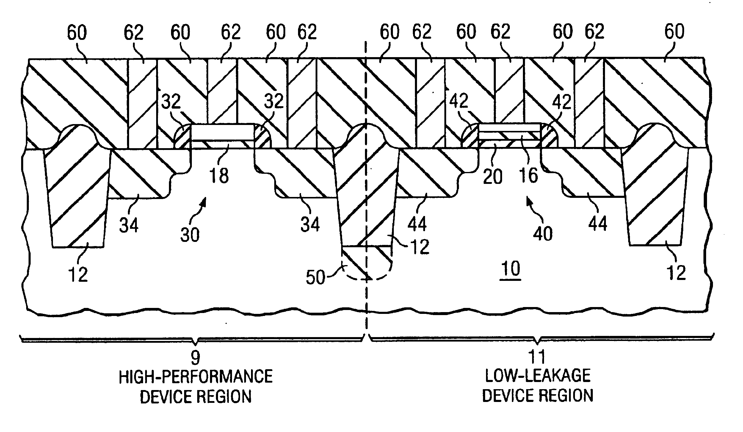
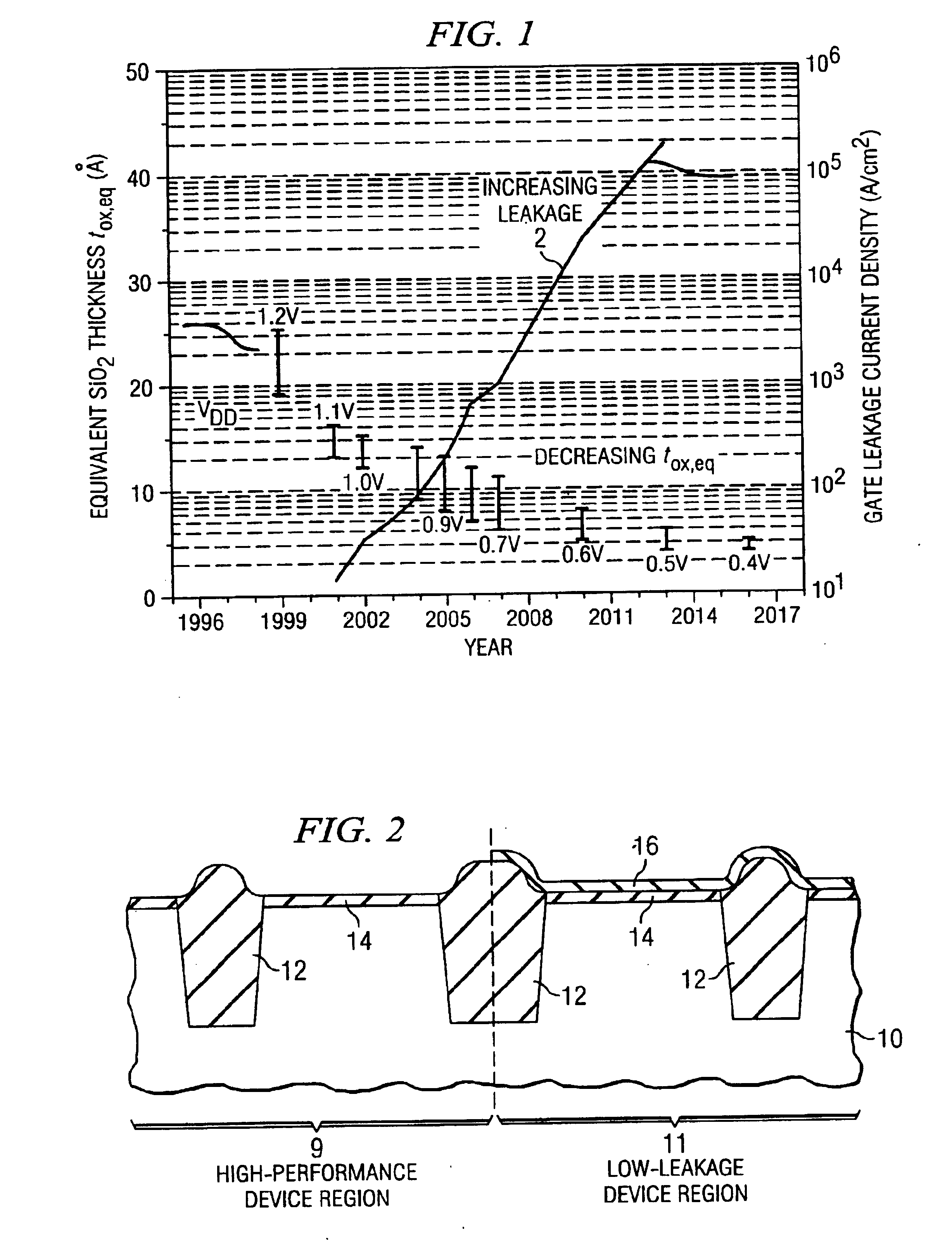
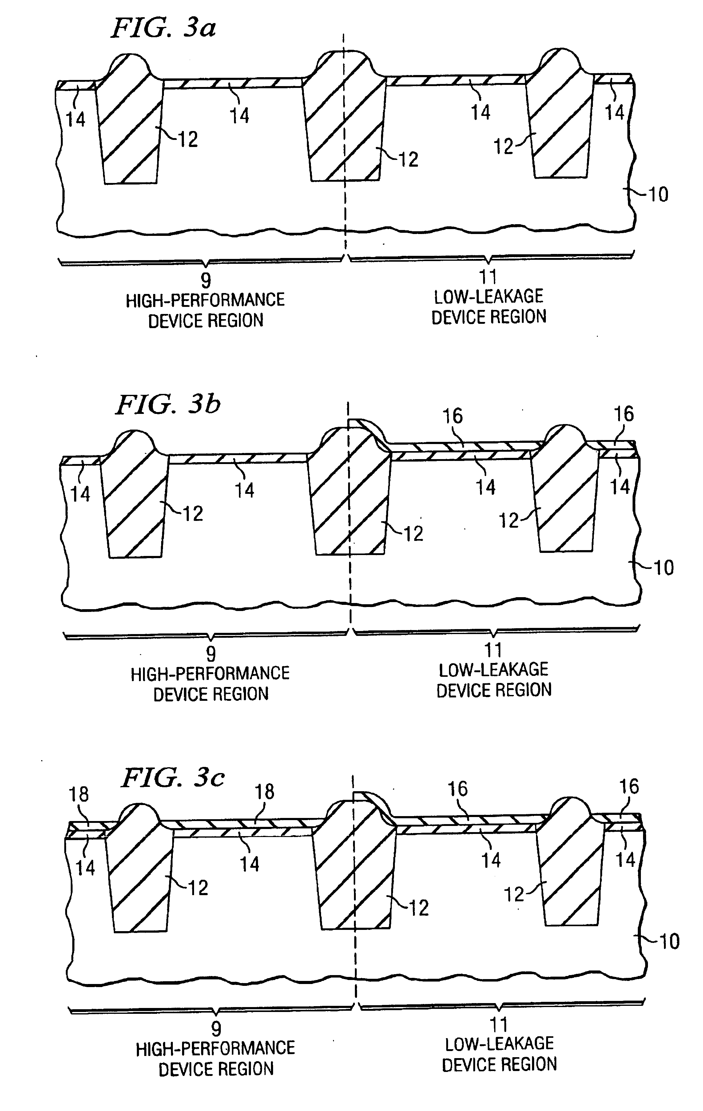
[0022]The making and using of the presently preferred embodiments are discussed in detail below. It should be appreciated, however, that the present invention provides many applicable inventive concepts that can be embodied in a wide variety of specific contexts. The specific embodiments discussed are merely illustrative of specific ways to make and use the invention, and do not limit the scope of the invention. For ease of reference, common reference numerals will be used throughout the figures when referring to the same or similar features common to the figures.

[0023]In the preferred embodiments of the present invention, at least two different gate dielectric materials are formed on a semiconductor chip to obtain both high-performance devices and low-leakage devices on the same chip. Preferably, a silicon oxide SiO2 or silicon oxynitride SiON gate dielectric is provided for high-performance devices, and another gate dielectric comprising a stacked high-k / SiO2 or high-k / SiON gate d...


PUM


Abstract

Both high performance and low leakage current devices can be formed on a single wafer without significant additional processing steps by the formation of an ultra-thin gate dielectric and a high-permittivity gate dielectric, respectively, in regions wherein switching speed and low leakage current, respectively, are desired. Logic and embedded memory regions can be performance optimized on the same integrated circuit.

Description

TECHNICAL FIELD[0001]The present invention relates generally to the field of semiconductor devices and more particularly to semiconductor chips having differing gate dielectrics in different regions of the chips and the methods for the manufacturing of same.BACKGROUND[0002]Size reduction of the metal-oxide-semiconductor field-effect transistor (MOSFET) has enabled the continued improvement in speed performance, density, and cost per unit function of integrated circuits over the past few decades. As the gate length of the conventional bulk MOSFET is reduced, it suffers from problems related to the inability of the gate to substantially control the on and off states of the channel. Phenomena such as reduced gate control associated with transistors with short channel lengths are termed short-channel effects. These short channel effects become particularly pronounced as device geometries shrink to 0.13 microns and below. One of the primary means by which short-channel effects are kept u...

Claims


Application Information

Patent Timeline
Patent Type & Authority Patents(United States)
IPC IPC(8): H01L21/70H01L21/8234H01L27/085H01L27/088
CPCH01L27/088H01L21/823462
Inventor YEO, YEE-CHIAYANG, FU-LIANGHU, CHENMING
Owner TAIWAN SEMICON MFG CO LTD
Why Eureka
Try Eureka