Measuring a property of a layer in multilayered structure
Inactive Publication Date: 2005-06-14
APPLIED MATERIALS INC
View PDF76 Cites 20 Cited by
Summary
Abstract
Description
Claims
Application Information
AI Technical Summary
This helps you quickly interpret patents by identifying the three key elements:
Problems solved by technology
Method used
Benefits of technology
[0021]In a second embodiment, the measurement apparatus computes a ratio (also called “steady-state ratio”) of the reflected power to the power of the heating beam and uses the ratio as a measure of the resistance per unit length of the conductive line. The second embodiment eliminates the need to perform at least two measurements that are otherwise required to determine a straight line, and is based on the fact that the refl
Problems solved by technology
Moreover, the above-described methods measure merely the resistivity of a metal film, and are not known to be u
Method used
Image
Click on the blue label to locate the original text in one second.
Reading with bidirectional positioning of images and text.
Examples
Embodiment Construction
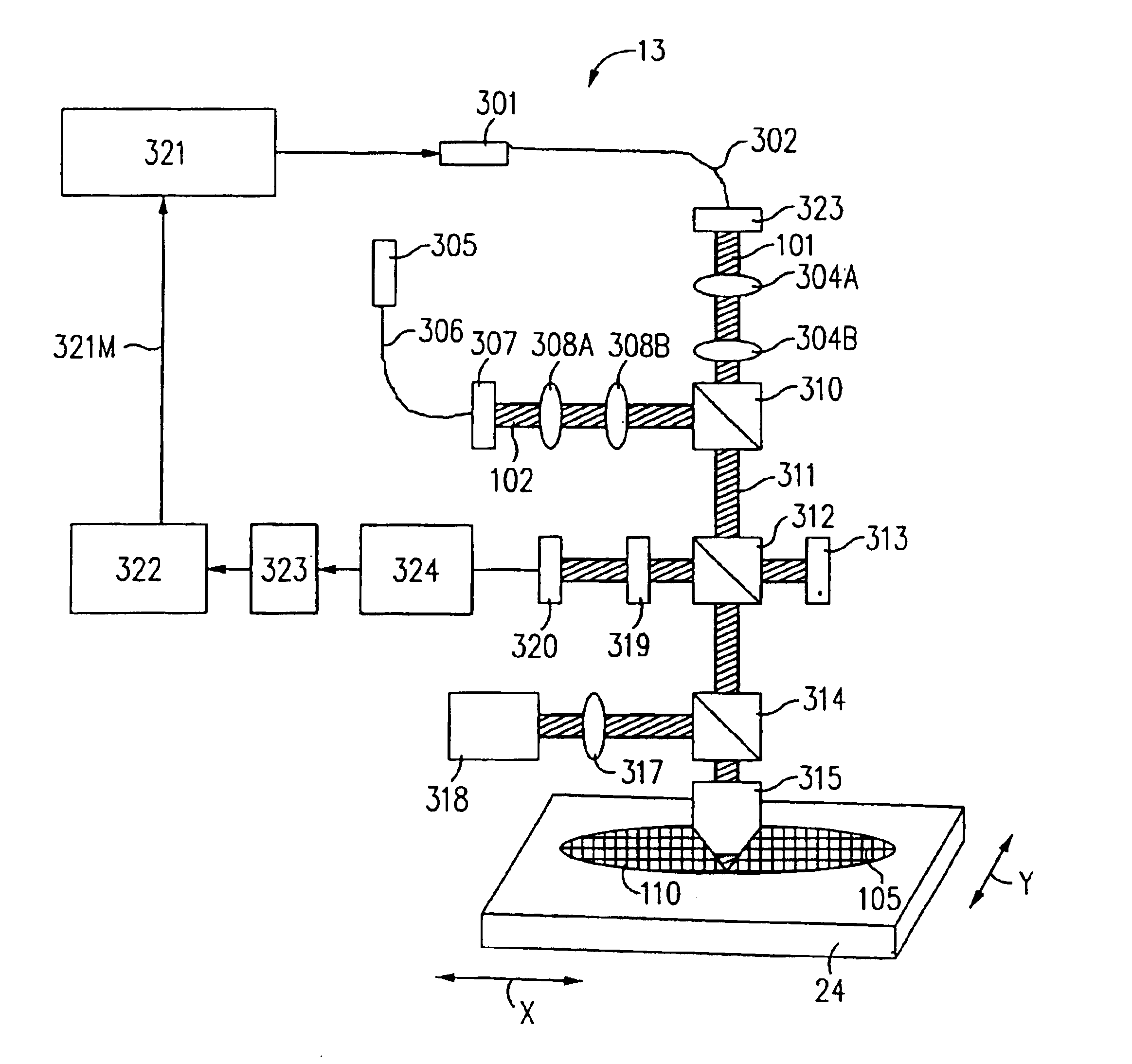
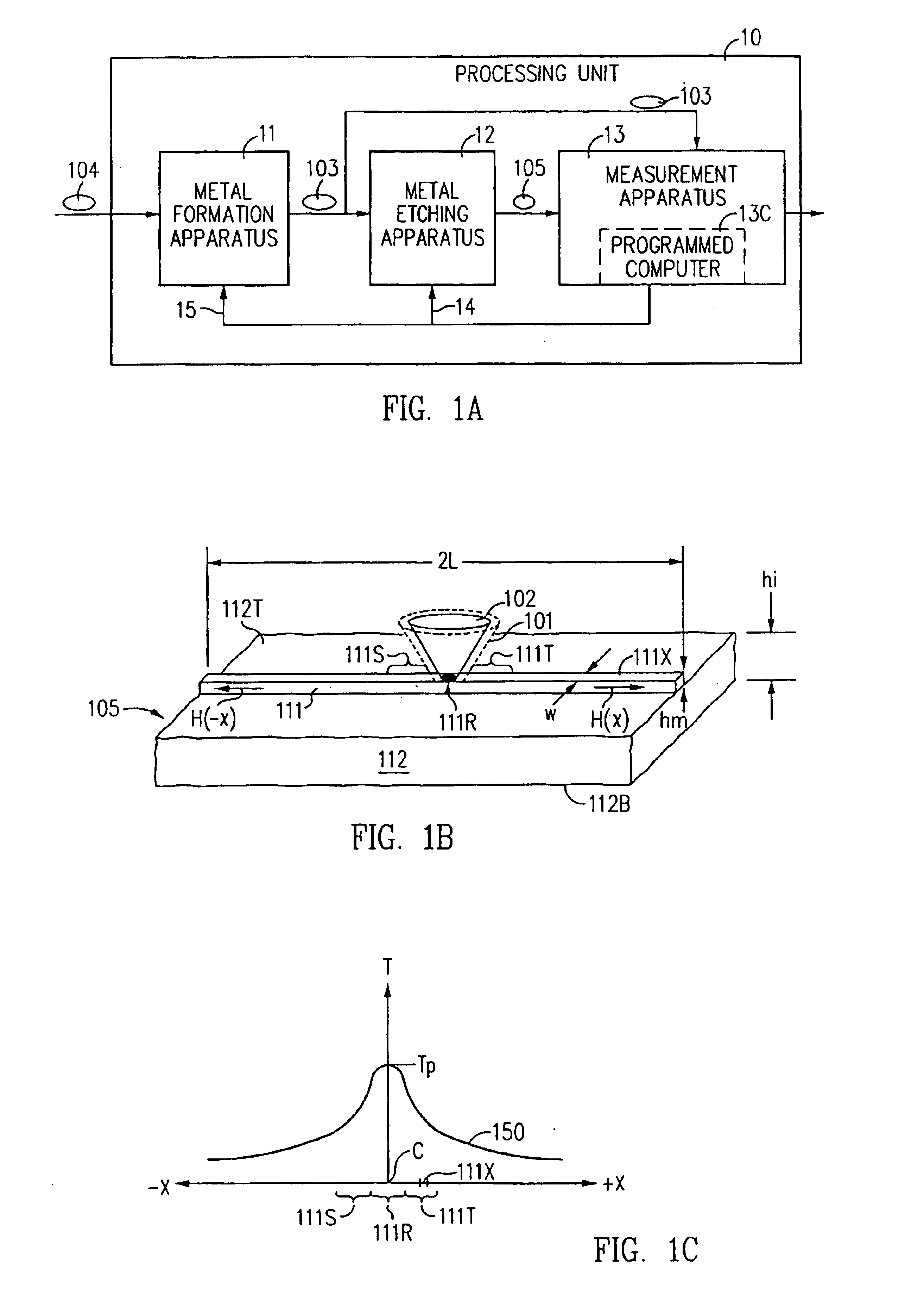
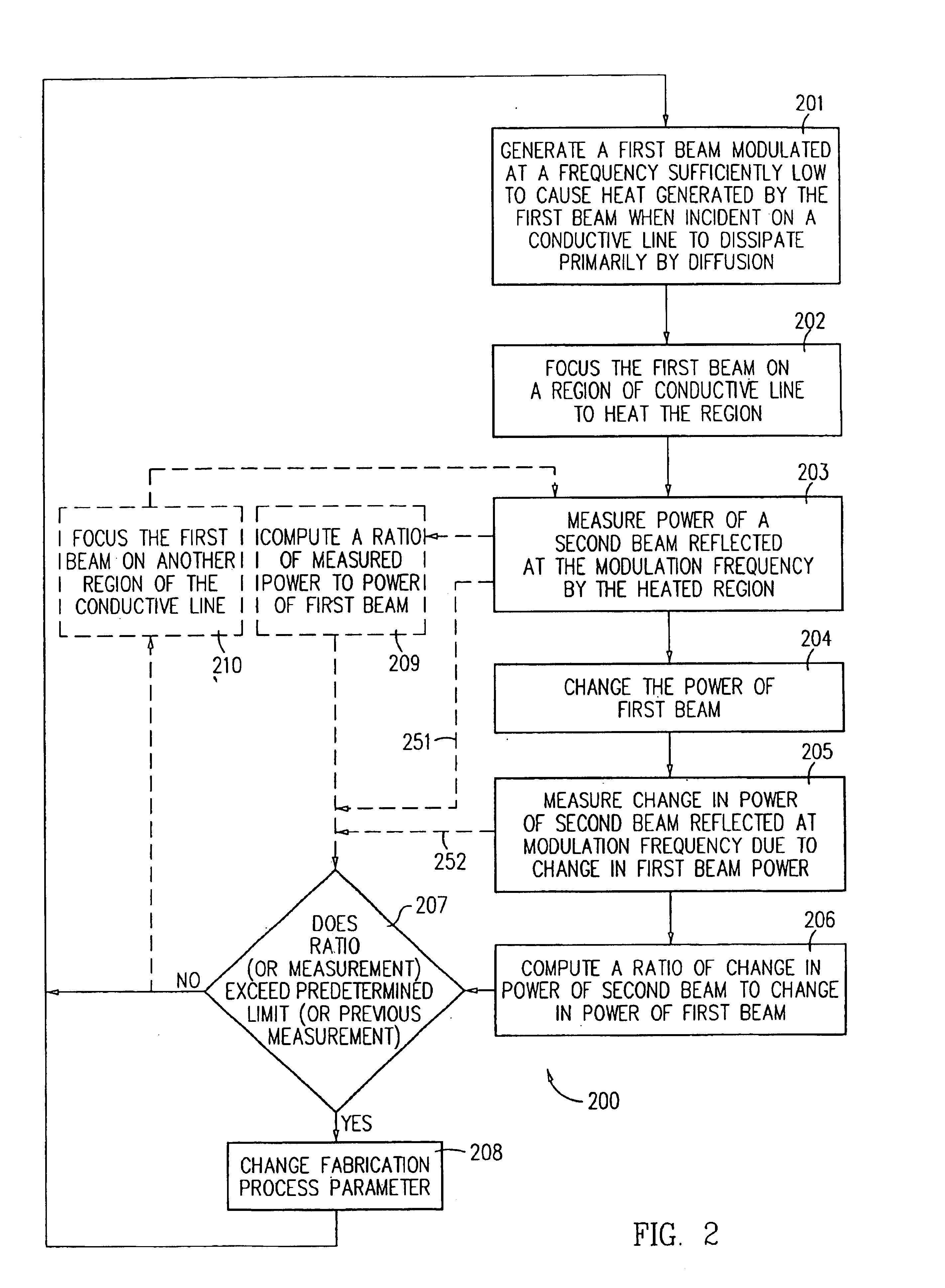
[0039]A processing unit 10 (FIG. 1A) can be operated in accordance with the invention to create integrated circuit (abbreviated as “IC”) dice by processing a substrate 104 to form a patterned substrate 105, measuring the resistance of one or more conductive lines in patterned substrate 105, and adjusting the processing in real time if necessary. Specifically, unit 10 includes a metal deposition apparatus 11 that forms on substrate 104 a layer of conductive material (such as a metal) to form a metallized wafer 103 that is in turn processed by metal etching apparatus 12 that etches the film to form one or more conductive lines in substrate 105. Unit 10 also includes a resistance measurement apparatus 13 that measures the resistance of one or more of the conductive lines (e.g. line 111 in FIG. 1B) on patterned substrate 105, or of one or more regions on unpatterned substrate 103 or both (i.e. before and after patterning of the same substrate).
[0040]If the resistance measurement falls o...
PUM
Abstract
An apparatus measures a property of a layer (such as the sheet resistance of a conductive layer or thermal conductivity of a dielectric layer that is located underneath the conductive layer) by performing the following method: (1) focusing the heating beam on the heated a region (also called “heated region”) of the conductive layer (2) modulating the power of the heating beam at a predetermined frequency that is selected to be sufficiently low to ensure that at least a majority (preferably all) of the generated heat transfers out of the heated region by diffusion, and (3) measuring the power of another beam that is (a) reflected by the heated region, and (b) modulated in phase with modulation of the heating beam. The measurement in act (3) can be used directly as a measure of the resistance (per unit length) of a conductive line formed by patterning the conductive layer. Acts (1)-(3) can be repeated during fabrication of a semiconductor wafer, at each of a number of regions on a conductive line, and any change in measurement indicates a corresponding change in resistance of the line. When the measurement changes by more than a predetermined amount (e.g. by 10%), a process parameter that controls the fabrication process is changed to return the measurement to normal in the next wafer. Moreover, the thermal conductivity of the dielectric layer can be measured, or monitored for changes beyond a predetermined limit during a scan across the wafer, if resistance is known.
Description
CROSS-REFERENCE TO RELATED APPLICATIONS[0001]This application is a continuation application of U.S. patent application Ser. No. 10 / 269,619 filed Oct. 11, 2002 now abandoned by Peter G. Borden, Regina G. Nijmeijer and Jiping Li, which is in turn a continuation of Ser. No. 09 / 544,280 filed Apr. 6, 2000 now issued as U.S. Pat. No. 6,489,801 which is itself a continuation of Ser. No. 09 / 095,804 filed Jun. 10, 1998 now issued as U.S. Pat. No. 6,049,220.[0002]This application presents the same material as presented in U.S. patent application Ser. No. 09 / 095,805 now U.S. Pat. No. 6,054,868, which was previously incorporated by reference in each of the applications identified in the previous paragraph.[0003]This application is also related to and incorporates by reference in their entirety each of the following commonly owned U.S. patent applications:[0004]Ser. No. 08 / 638,944, filed Apr. 24, 1996, now U.S. Pat. No. 5,883,518;[0005]Ser. No. 08 / 637,244, filed Apr. 24, 1996, now U.S. Pat. No 5...
Claims
Application Information
Patent Timeline
Application Date:The date an application was filed.
Publication Date:The date a patent or application was officially published.
First Publication Date:The earliest publication date of a patent with the same application number.
Issue Date:Publication date of the patent grant document.
PCT Entry Date:The Entry date of PCT National Phase.
Estimated Expiry Date:The statutory expiry date of a patent right according to the Patent Law, and it is the longest term of protection that the patent right can achieve without the termination of the patent right due to other reasons(Term extension factor has been taken into account ).
Invalid Date:Actual expiry date is based on effective date or publication date of legal transaction data of invalid patent.